Pinned photodiode (PPD) pixel with high shutter rejection ratio for snapshot operating CMOS sensor

a photodiode and shutter rejection ratio technology, applied in the field of solid-state image sensing devices, can solve the problems of complicated control of this type of read-out, motion artifacts, and distortion of images, and achieve the effects of preventing the generation of photoelectrons, preventing the leakage of substrate charge, and preventing the formation of substrate charg

Active Publication Date: 2008-09-09
GULA CONSULTING LLC
View PDF15 Cites 8 Cited by
  • Summary
  • Abstract
  • Description
  • Claims
  • Application Information

AI Technical Summary

Benefits of technology

[0027]Another object of this invention is to provide a pixel image sensor that prevents substrate charge leakage to a floating diffusion storage node of the pixel image sensor.
[0028]Further, another object of this invention is to provide a pixel image sensor that prevents generation of photoelectrons within the floating diffusion storage node and storage node control transistor switches of the pixel image sensor;
[0029]Even further, another object of this invention is to provide a pixel image sensor that prevents substrate charge leakage of photoelectrons from pixel image sensor adjacent to the pixel image sensor.
[0030]To accomplish at least one of these objects, a pixel image sensor is fabricated on a substrate. An isolation barrier is placed at a relatively great depth from a surface of the substrate and beneath a floating diffusion storage node and storage node control transistor switches of the pixel image sensor to prevent substrate charge leakage caused by photoelectrons generated in the substrate beneath a photon sensing area of the pixel image sensor from drifting to the storage node. A diffusion well is placed in the surface of the substrate to contact the isolation barrier and connected to a first biasing voltage to channel the photoelectrons away from the storage node. A carrier conduction well is placed at the relatively great depth and adjoining the isolation barrier to channel the substrate charge leakage to the isolation barrier. The carrier conduction well contains a photo sensing region of the pixel image sensor. The photo sensing region of the pixel image sensor is a pinned photodiode that is formed within the carrier conduction well.
[0031]A metal shield is fabricated above the storage node and storage node control transistor switches to prevent light from impinging on the storage node and storage node control transistor switches. The metal shield prevents generation of photoelectrons at the storage node and storage node control transistor switches. In the preferred embodiment, the metal shield is a combination of interconnecting wiring, interlayer vias, and substrate contact metallurgy placed above the storage node and storage node control transistor switches.
[0032]A metallic silicide is optionally placed in contact with the storage node and source / drain regions of the storage node control transistor switches. The metallic silicide layer being opaque, prevents light impinging on the storage node and storage node control transistor switches from generation of photoelectrons at the storage node and storage node control transistor switches.

Problems solved by technology

The stray photoelectrons 64 then cause noise currents that interfere with the detection of the correct values of light intensity and cause distortion such as blooming and smearing of the image.
This technique has minimum integration time to collect the photons and minimum time for generating a frame, however it may have motion artifacts due to non-simultaneous exposure.
Control for this type of read out is complicated
The non-simultaneous exposure of the pixels can lead to image distortion, for example, when there is relative motion between the imager and the image that is to be captured.
Transfer of such unwanted charges into the sense node can result in image distortion and excess noise.
Furthermore, the distortions tend to become more pronounced as the exposure time is reduced.
However, relatively long integration times (10 msec) precludes the capture of high velocity moving objects without blurring or the motion artifact.

Method used


Image

  • Pinned photodiode (PPD) pixel with high shutter rejection ratio for snapshot operating CMOS sensor
  • Pinned photodiode (PPD) pixel with high shutter rejection ratio for snapshot operating CMOS sensor
  • Pinned photodiode (PPD) pixel with high shutter rejection ratio for snapshot operating CMOS sensor

Examples


Embodiment Construction

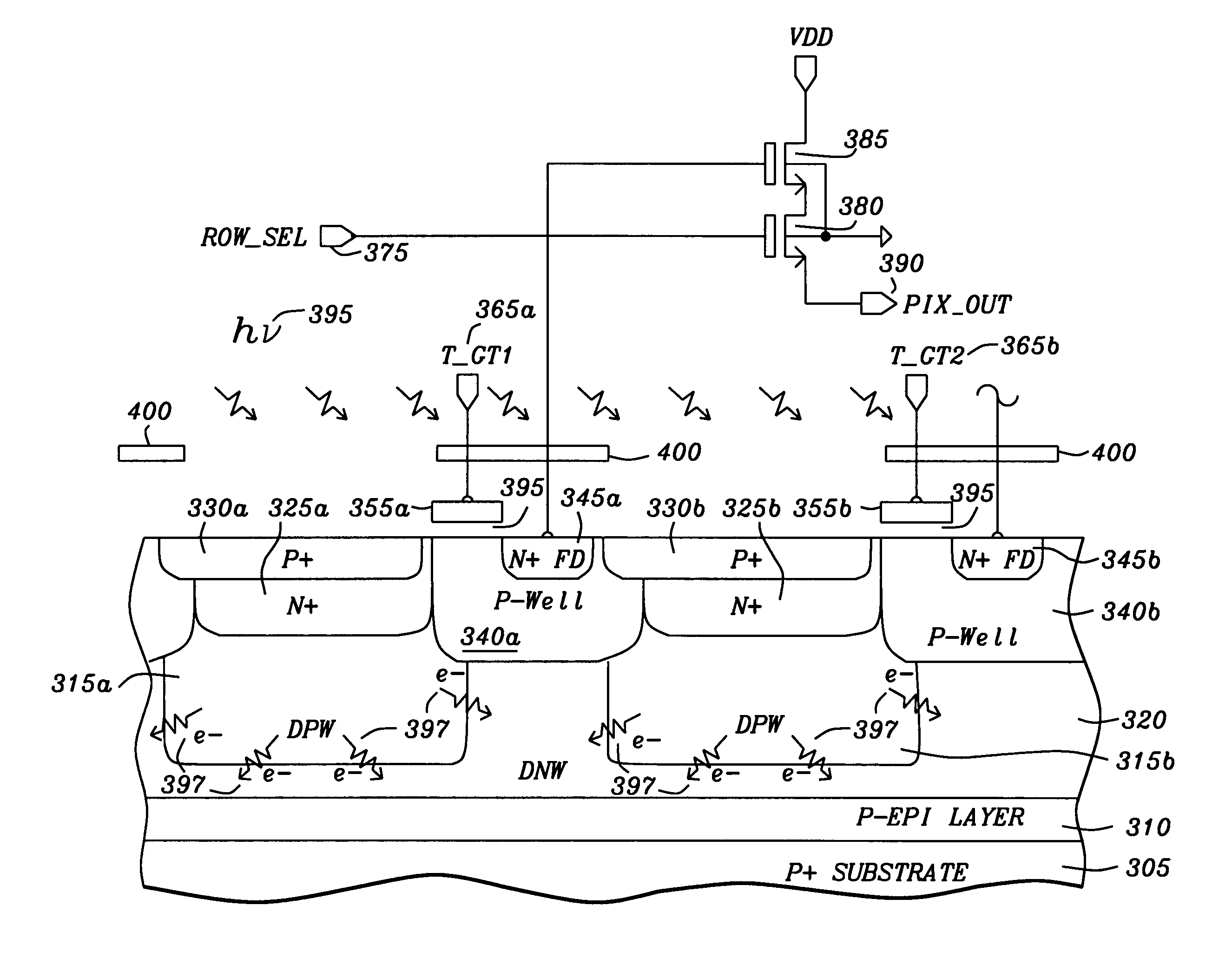
[0042]Camera systems that are intended for capturing fast moving images require arrays of snapshot CMOS active pixel image sensors with an ultra high light shutter rejection ratio for detecting moving objects without motion artifacts. Light leakage to the storage node must be minimized to provide snapshot images without motion artifacts.

[0043]Refer to FIG. 2 for a discussion of an image processing application specific integrated circuit 150. The image processing application specific integrated circuit contains an image sensor 100. The image sensor 100 has an array 105 of snapshot pinned photodiode CMOS active pixel image sensors, row control circuitry 110, column sample and hold circuitry 115, a video amplifier 120, and an analog-to-digital converter 125.

[0044]The image processing application specific integrated circuit 150 has pinned photodiode active pixel image sensor array 105 with a few rows of dark pixels for auto offset correction. In the particular intended application as a ...


PUM


Abstract

A pixel image sensor has a high shutter rejection ratio that prevents substrate charge leakage to a floating diffusion storage node of the pixel image sensor and prevents generation of photoelectrons within the floating diffusion storage node and storage node control transistor switches of the pixel image sensor. The pixel image sensor that prevents substrate charge leakage of photoelectrons from pixel image sensor adjacent to the pixel image sensor. The pixel image sensor is fabricated on a substrate with an isolation barrier and a carrier conduction well. The isolation barrier formed underneath the floating diffusion storage node allows effective isolation by draining away the stray carriers and preventing them from reaching the floating diffusion storage node. The carrier conduction well in combination with the deep N-well isolation barrier separates the pinned photodiode region from the deep N-well isolation barrier that is underneath the floating diffusion storage node.

Description

BACKGROUND OF THE INVENTION[0001]1. Field of the Invention[0002]The present invention relates to solid-state image sensing devices, methods for fabricating solid state image sensing devices and an image capture system using the same.[0003]2. Description of Related Art[0004]Integrated circuit image sensors are finding applications in a wide variety of fields, including machine vision, robotics, guidance and navigation, automotive applications, and consumer products such as digital camera and video recorders. Imaging circuits typically include a two dimensional array of photo sensors. Each photo sensor includes one picture element (pixel) of the image. Light energy emitted or reflected from an object impinges upon the array of photo sensors. The light energy is converted by the photo sensors to an electrical signal. Imaging circuitry scans the individual photo sensors to readout the electrical signals. The electrical signals of the image are processed by external circuitry for subsequ...

Claims


Application Information

Patent Timeline
Patent Type & Authority Patents(United States)
IPC IPC(8): H01L31/062H01L31/113
CPCH01L27/14609H01L27/1463H01L27/14689
Inventor DOSLUOGLU, TANERYANG, GUANG
Owner GULA CONSULTING LLC
Why Eureka
Try Eureka