Nanowhiskers with pn junctions, doped nanowhiskers, and methods for preparing them

a nanowhisker and junction technology, applied in nanoinformatics, nanocontrolling devices, crystal growth processes, etc., can solve the problems of reducing the mobility of carriers, reducing the junction quality of nanowires, and affecting the conductivity of carriers, so as to improve the conductivity characteristics

Inactive Publication Date: 2008-10-07
QUNANO
View PDF43 Cites 28 Cited by
  • Summary
  • Abstract
  • Description
  • Claims
  • Application Information

AI Technical Summary

Benefits of technology

[0031]In a further aspect, a nanowhisker or other one-dimensional nanoelement is surrounded by a material containing dopant ions. For example the surrounding material may be a polymer material. By a process, for example a subsequent step of rapid thermal annealing, the dopant ions in the matrix material are permitted themselves to diffuse into the nanowhisker, to create a desired conductivity. This provides advantages over a direct doping into the nanoelement, by providing an extra degree of control over the doping process, and permitting the diffusion of certain dopants into the nanoelement that would not be possible by a more direct process. Although a polymer material is preferred, which is evaporated or spun onto a substrate so as to surround the nanowhisker, other materials may be employed, such as for example semiconductor material or dielectric material grown onto the substrate. The dopant material may be incorporated in the surrounding material before application to the substrate, during the application to the substrate, or as a subsequent step after the surrounding material is formed on the substrate.
[0046]The invention recognises that for a one-dimensional nanoelement, where there may be a wide range of possibilities to combine III-V semiconductors in spite of lattice mismatch, Fermi Level Pinning is a constructive way to make pn-junctions by choosing semiconductor alloy composition to determine carrier type. In such devices the band gap can be engineered and the carrier type can be controlled to make new types of semiconductor devices. When a semiconductor crystal ends abruptly at an interface, and “band bending” tends to occur to equalize the Fermi Levels on the two sides of the interface, Fermi Level Pinning, arising from the existence of surface trap states, counteracts this effect to reduce the amount of charge transfer across the interface.

Problems solved by technology

This may result in structures ranging in size from small devices of atomic dimensions, to much larger scale structures for example on the microscopic scale.
In general, there are problems in that the definition of the junction within the nanowire is not good enough for electrical components, and in that the presence of dopant ions within the crystal creates crystal imperfections and reduces carrier mobility.
A difficulty with this approach is the extra step required of physically positioning the nanowires.

Method used


Image

  • Nanowhiskers with pn junctions, doped nanowhiskers, and methods for preparing them
  • Nanowhiskers with pn junctions, doped nanowhiskers, and methods for preparing them
  • Nanowhiskers with pn junctions, doped nanowhiskers, and methods for preparing them

Examples


first embodiment

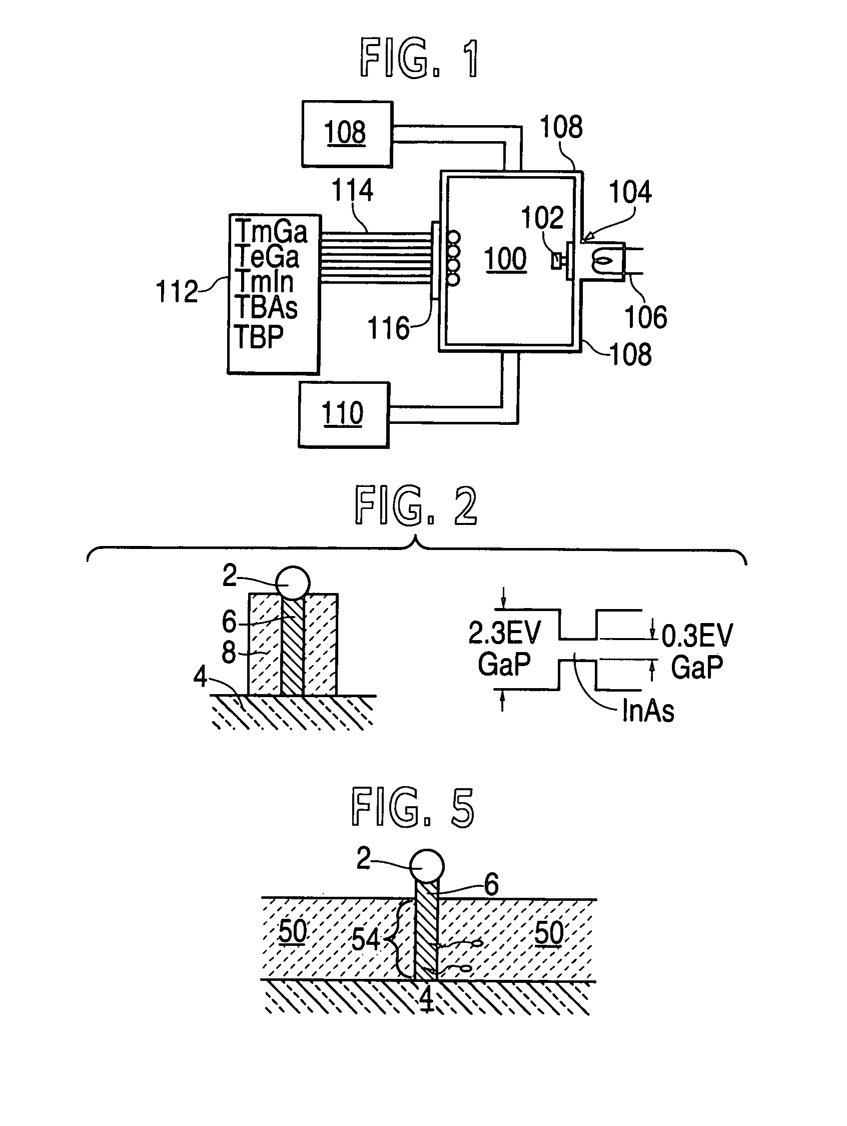
[0075]Referring now to FIG. 2, the invention is formed by positioning a gold aerosol particle 2 on a III-V substrate 4, e.g., a gallium arsenide substrate. With appropriate conditions of temperature and pressure a nanowhisker of indium arsenide is grown by injecting organic materials TMIn and TBAs in a conventional VLS procedure, e.g., in a chemical beam epitaxial method, using the apparatus described above, or by a metal organic vapor phase epitaxy (MOVPE), or the like. Indium and arsenide ions are absorbed in the gold particle 2 and supersaturation conditions create a solid pillar 6 of indium arsenide.

[0076]Once the indium arsenide whisker has been grown, different materials TEGa and TBP are used to create a coaxial jacket or surrounding layer 8 of GaP around the nanowhisker 6. Layer 8 may be created by CBE; using the apparatus of FIG. 1, wherein the conditions of temperature (106) and / or pressure (112) are changed to inhibit growth by the VLS mechanism, and instead to support bul...

second embodiment

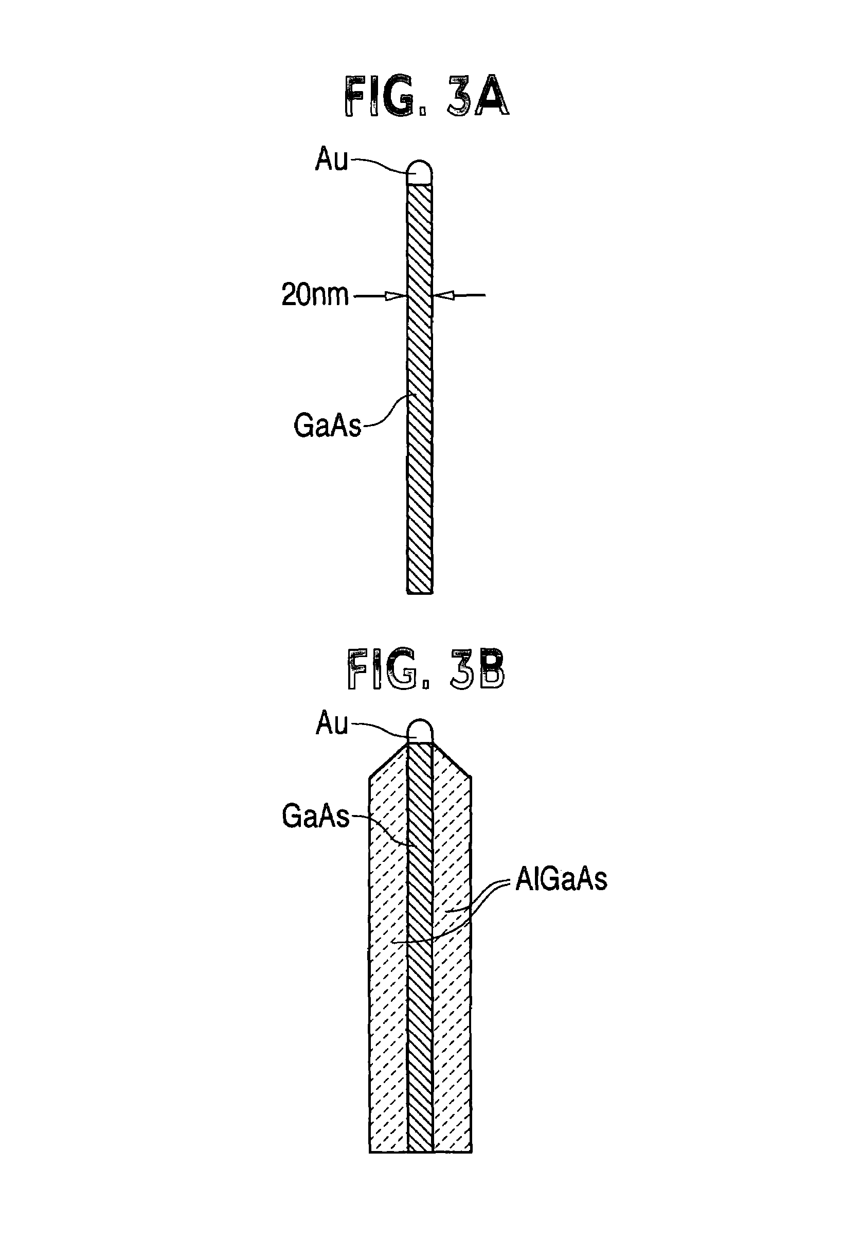
[0088]Referring now to FIG. 4 there is shown the invention. Similar parts to those of FIG. 2 are identified by the same reference numeral. A structure is produced comprising an inner nanowhisker of GaAs material 6, produced from a catalytic particle 2. The whisker is surrounded by a coaxial jacket 8 of AlGaAs. Then, first and second layers 20, 22 are provided, being of polymer or glass material spun on to the surface of substrate 4. Layer 20 contains n type dopant ions 24, and layer 22 contains p type dopant ions 26. A rapid thermal annealing step ensures that dopant ions 24, 26 migrate into corresponding regions 28, 30 of coaxial jackets 8. The annealing step is controlled such that there is no appreciable diffusion into the nanowhisker 6.

[0089]The result is that the dopant ions within regions 28, 30 create corresponding regions 32, 34 within nanowhisker 6 by modulation doping of opposite conductivity type. These regions that are stable space charge regions create a region 36 deple...

third embodiment

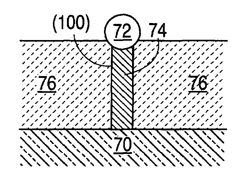
[0091]Referring now to FIG. 5, there is shown the invention, wherein similar parts to those of FIG. 2 are denoted by the same reference numeral. Thus an indium arsenide nanowhisker 6 is grown on a gallium arsenide substrate 4 by chemical beam epitaxy employing a gold catalytic particle 2.

[0092]After formation of the nanowhisker, a first layer 50 of polymer material is evaporated (preferred) or spun onto the substrate 4. There is commercially available a wide range of dielectric materials formed of carbon or silicon based polymers, some of which are doped and have defined electrical conductivity characteristics. The polymer material has contained within it a desired concentration of dopant ions of a desired type. As may be seen, layer 50 extends towards the top of the nanowhisker. The depth of layer 50 can be determined very accurately with evaporation of polymer.

[0093]The entire structure is then subject to rapid thermal annealing. This permits the dopant ions in the polymer materia...


PUM

PropertyMeasurementUnit
thicknessaaaaaaaaaa
diameteraaaaaaaaaa
thickaaaaaaaaaa

Abstract

Nano-engineered structures are disclosed, incorporating nanowhiskers of high mobility conductivity and incorporating pn junctions. In one embodiment, a nanowhisker of a first semiconducting material has a first band gap, and an enclosure comprising at least one second material with a second band gap encloses said nanoelement along at least part of its length, the second material being doped to provide opposite conductivity type charge carriers in respective first and second regions along the length of the of the nanowhisker, whereby to create in the nanowhisker by transfer of charge carriers into the nanowhisker, corresponding first and second regions of opposite conductivity type charge carriers with a region depleted of free carriers therebetween. The doping of the enclosure material may be degenerate so as to create within the nanowhisker adjacent segments having very heavy modulation doping of opposite conductivity type analogous to the heavily doped regions of an Esaki diode. In another embodiment, a nanowhisker is surrounded by polymer material containing dopant material. A step of rapid thermal annealing causes the dopant material to diffuse into the nanowhisker. In a further embodiment, a nanowhisker has a heterojunction between two different intrinsic materials, and Fermi level pinning creates a pn junction at the interface without doping.

Description

CROSS-REFERENCE TO RELATED APPLICATIONS[0001]This application claims the benefit of the priority of U.S. Provisional Patent Application No. 60 / 459,990 filed Apr. 4, 2003, the entirety of which is incorporated herein by reference.BACKGROUND OF THE INVENTION[0002]1. Field of the Invention[0003]This invention relates generally to structures and devices produced by techniques of nanotechnology.[0004]More specifically, the invention relates to such structures and devices incorporating at least one element, essentially in one-dimensional form, and that is of nanometer dimensions in its width or diameter, and that preferably is produced by the so-called Vapor-Liquid-Solid (VLS) mechanism. For the purposes of this specification, such element will be termed a “nanowhisker”.[0005]2. Brief Description of the Prior Art[0006]Nanotechnology covers various fields, including that of nanoengineering, which may be regarded as the practice of engineering on the nanoscale. This may result in structures...

Claims


Application Information

Patent Timeline
Patent Type & Authority Patents(United States)
IPC IPC(8): H01L29/06C30B11/00C30B11/12H01L21/205H01L21/225H01L29/861H01L29/885
CPCB82Y10/00C30B11/00C30B11/12H01L21/02395H01L21/02461H01L21/02463H01L21/02543H01L21/02546H01L21/02573H01L21/02603H01L21/0262H01L21/02631H01L21/02653H01L21/2258H01L29/0665H01L29/0673H01L29/0676H01L29/068H01L29/861H01L29/885C30B29/62Y10S977/932B82Y20/00H01L29/06
Inventor SAMUELSON, LARS IVAROHLSSON, BJORN JONASLEDEBO, LARS-.ANG.KE
Owner QUNANO
Why Eureka
Try Eureka