Light emitting device with filled tetrahedral (FT) semiconductor in the active layer

a technology of filling tetrahedron and active layer, which is applied in the direction of semiconductor lasers, discharge tubes luminescnet screens, natural mineral layered products, etc., can solve the problems of poor lower thermal stability, thermal instability, and semiconductors containing ft semiconductors

Inactive Publication Date: 2008-11-04
KK TOSHIBA
View PDF2 Cites 8 Cited by
  • Summary
  • Abstract
  • Description
  • Claims
  • Application Information

AI Technical Summary

Problems solved by technology

However, the rare gas-containing FT semiconductor or molecule-containing FT semiconductor proposed by Rompa et al. is believed to be thermally unstable because the inserted substance can move within the crystal and, thus, not to be suitable for practical use.
Under the circumstances, it can be easily expected that the rare gas-containing FT semiconductor or molecule-containing FT semiconductor, which can certainly form the FT structure, may be poor in lower thermal stability.
In short, there is a problem that the FT semiconductor will not be a practical material system.
However, there is a problem that the FT semiconductor in which a closed-shell substance such as a rare gas atom or diatomic molecule is inserted into the interstitial site is poor in thermal stability and is not practical because the closed-shell substance is not chemically bonded with the matrix semiconductor.

Method used


Image

  • Light emitting device with filled tetrahedral (FT) semiconductor in the active layer
  • Light emitting device with filled tetrahedral (FT) semiconductor in the active layer
  • Light emitting device with filled tetrahedral (FT) semiconductor in the active layer

Examples


first embodiment

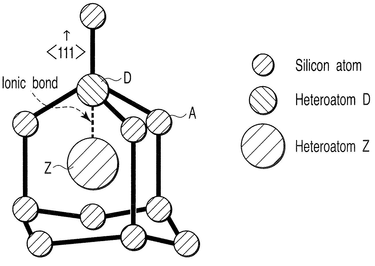
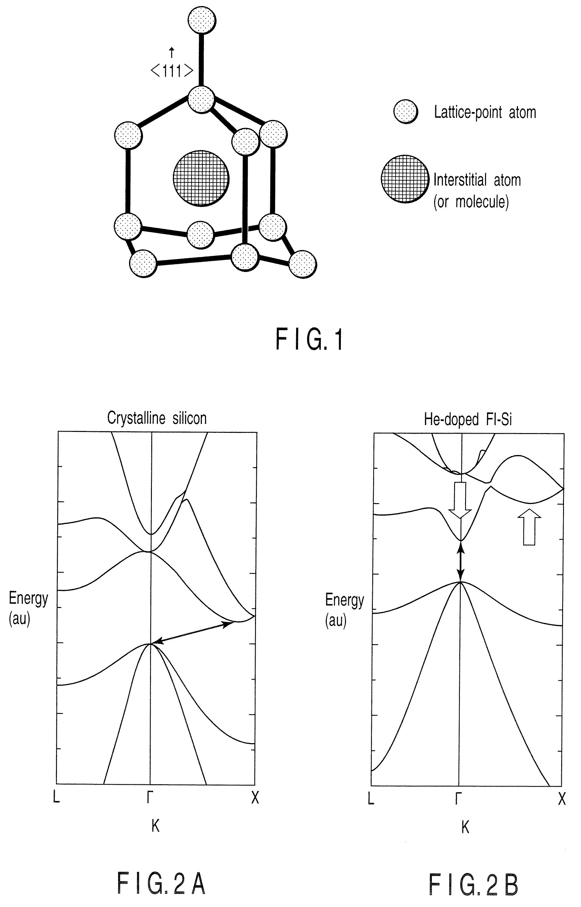
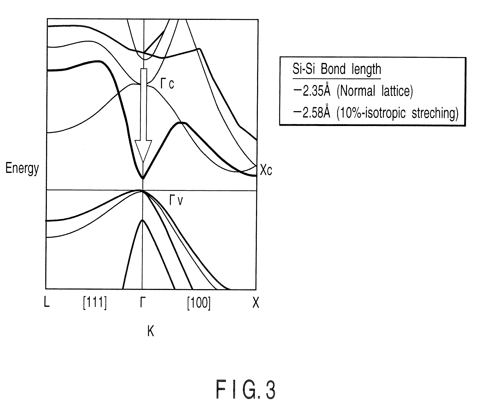
[0103]A silicon light emitting device of the vertical type, which is constructed as shown in FIG. 9A, will be described. The PF doped FT-Si active layer is formed by using silicon as the matrix semiconductor, the P atom as the heteroatom D substituted for the lattice site, and the F atom as the heteroatom Z inserted into the interstitial site. The PF pair concentration is 2.5×10²⁰ / cm3. The concentration of each of the P atoms and the F atoms can be confirmed by SIMS.

[0104]For examining whether a PF pair of a pendant type FT structure is formed in the active layer, it is effective to examine the vibration mode inherent in the PF pair, and the PF pair can be detected by the microspectroscopy of the active layer. As a method of easily checking the PF pair formation, it is possible to prepare a PF-doped region having a composition equal to that of the active layer and a region doped with P alone on the surface of a substrate having a high resistivity so as to compare these two doped reg...

second embodiment

[0112]A light emitting device of the structure equal to that of the first embodiment is prepared except that the B atom of a p-type dopant is used as the heteroatom D and the K atom is used as the heteroatom Z. Each of the B concentration and the K concentration as determined by SIMS is 5×10²⁰ / cm3, and the BK pair concentration is estimated at 5×10²⁰ / cm3.

[0113]When the light emitting device is excited with light, PL emission is caused at the wavelength in the vicinity of the band gap of the crystalline silicon. When the element is driven with current, it is possible to bring about a current injection radiation from the region of the FT structure in the active layer. The emission wavelength is also equal to the wavelength in the vicinity of the band gap of the crystalline silicon, and the emitted light exhibits emission spectrum of a shape resembling the PL emission spectrum.

[0114]As apparent from the second embodiment, the light emitting function can be imparted to the indirect semi...

third embodiment

[0115]Light emitting devices are manufactured as in the first embodiment by using various materials as the matrix semiconductor, the heteroatom D at the lattice site and the heteroatom Z at the interstitial site.

[0116]Table 1 shows (1) the matrix semiconductor in the active layer, (2) the lattice site substituted by the heteroatom D, (3) the heteroatom D substituted for the lattice site, (4) the heteroatom Z inserted into the interstitial site, (5) the DZ pair concentration estimated from the Z concentration, and (6) the emission peak wavelength through current injection.

[0117]As shown in Table 1, emission through the current injection is caused even in compound indirect semiconductors by introducing a pendant type FT structure into the compound-based indirect semiconductor.

[0118]

TABLE 1(2)(5)(6)(1)Lattice siteDZ pairEmissionMatrixsubstituted by D(3)(4)concentrationwavelengthsemiconductor(group)D (group)Z (group)( / cm3)(nm)AlPP (15)Si (14)Na (1)1.5E+20515GaPGa (13)Mg (2)Na (1)2.1E+20...


PUM

PropertyMeasurementUnit
frequencyaaaaaaaaaa
wavelengthaaaaaaaaaa
frequencyaaaaaaaaaa

Abstract

A light emitting device includes an active layer including atoms A of a matrix semiconductor having a tetrahedral structure, a heteroatom D substituted for the atom A in a lattice site, and a heteroatom Z inserted into an interstitial site positioned closest to the heteroatom D, the heteroatom D having a valence electron number differing by +1 or −1 from that of the atom A, and the heteroatom Z having an electron configuration of a closed shell structure through charge compensation with the heteroatom D, and an n-electrode and a p-electrode adapted to supply a current to the active layer.

Description

CROSS-REFERENCE TO RELATED APPLICATIONS[0001]This application is based upon and claims the benefit of priority from prior Japanese Patent Application No. 2005-346601, filed Nov. 30, 2005, the entire contents of which are incorporated herein by reference.BACKGROUND OF THE INVENTION[0002]1. Field of the Invention[0003]The present invention relates to a light emitting device based on a filled tetrahedral (FT) semiconductor.[0004]2. Description of the Related Art[0005]In recent years, active research is being conducted on band engineering for modulating optical characteristics peculiar to a substance, such as emission and absorption, by modulating the energy band structure that has been considered to be inherent in the substance.[0006]For example, a quantum dot (or a quantum wire or a superlattice) and a strain effect are well known as a typical band engineering technique. The quantum dot (or the quantum wire or the superlattice) brings about a modulated band structure by reducing the s...

Claims


Application Information

Patent Timeline
Patent Type & Authority Patents(United States)
IPC IPC(8): H01L27/15H01L33/08H01L33/30H01L33/34H01L33/46H01L33/50
CPCB82Y20/00H01L33/26H01S5/22H01S5/3224H01S5/3412
Inventor YAMAMOTO, KAZUSHIGESHIMIZU, TATSUOHANEDA, SHIGERU
Owner KK TOSHIBA
Why Eureka
Try Eureka