Air gap for dual damascene applications

a damascene and air gap technology, applied in the field of integrated circuits, can solve the problems of increasing slowing circuit speeds, and negatively affecting overall device performance, so as to reduce manufacturing complexity and costs, improve manufacturing efficiency, and facilitate manufacturing and compatibility.

Inactive Publication Date: 2008-11-11
UNITED MICROELECTRONICS CORP
View PDF57 Cites 54 Cited by
  • Summary
  • Abstract
  • Description
  • Claims
  • Application Information

AI Technical Summary

Benefits of technology

[0017]It is an advantage of the present invention that the low dielectric constant of air is used to provide maximum electrical isolation by extending the air gap both below and above the adjacent isolated interconnects, or metal lines, while still ensuring that physical dielectric support is provided beneath the interconnects themselves.
[0018]It is a further advantage of the present invention that the air gap isolation structure is readily manufacturable and compatible with existing semiconductor manufacturing techniques.
[0019]It is a still further advantage of the present invention that exotic low K dielectric materials need not be used, thus saving costs and minimizing manufacturing complexity.
[0020]It is a still further advantage of the present invention that the existence of the air gaps is to release most of the system stress generated by subsequent thermal treatments.
[0021]It is a still further advantage of the present invention that the network structure using conventional dielectric layers encompassing the interconnects provides good thermal dissipation.

Problems solved by technology

The increased capacitive coupling results in increased parasitic capacitance, which undesirably slows circuit speeds and negatively impacts overall device performance.
While these materials have a relatively low dielectric constant, they are not normally used in semiconductor manufacturing and therefore increase manufacturing complexity and costs.
Some disadvantages of current low K materials include incompatible thermal coefficient of expansion, low mechanical strength and poor thermal diffusivity.
Previous attempts at air gap structures were hard to manufacture and also did not completely isolate adjacent metal lines due to fringing fields above and below the air gap itself.
This is both inefficient and imprecise for extremely small geometries.
This technique is clearly not suitable for precise control of air gap sizes, and is further disadvantageous because it cannot be used to form gaps which extend above a metal line.
Clearly, while portions of the aforementioned references are useful in forming air gap structures, and could be used in many applications, their overall approach is not optimal from a manufacturing perspective.

Method used


Image

  • Air gap for dual damascene applications
  • Air gap for dual damascene applications
  • Air gap for dual damascene applications

Examples


first embodiment

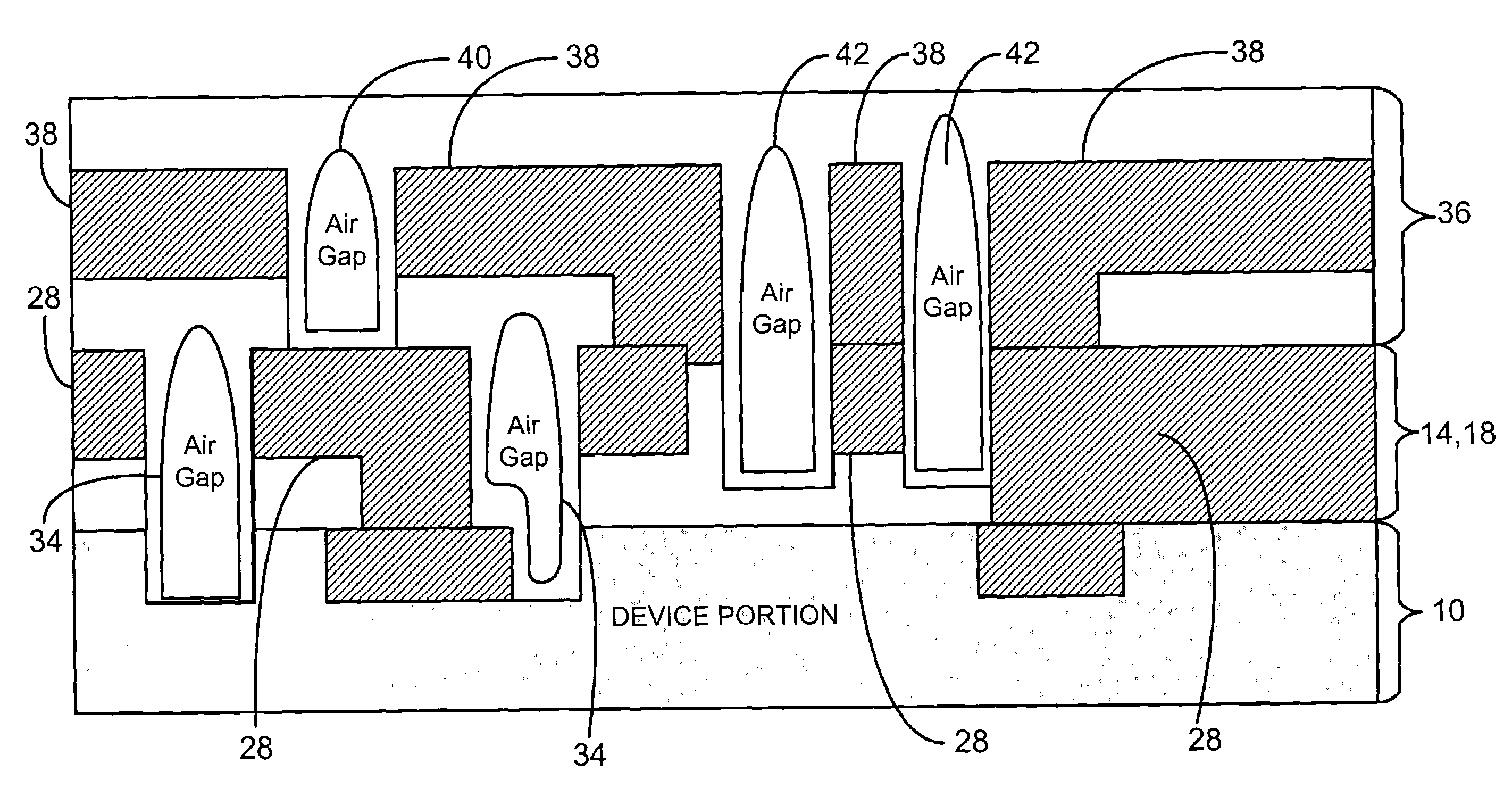
[0030]Referring generally now to FIGS. 1-13, a method for forming an integrated circuit device having an air gap structure is shown for a dual damascene—type metal interconnect structure.

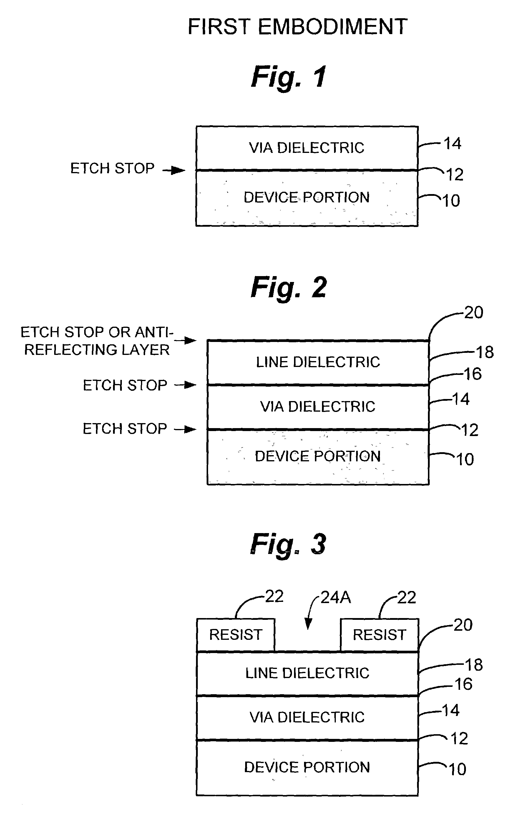
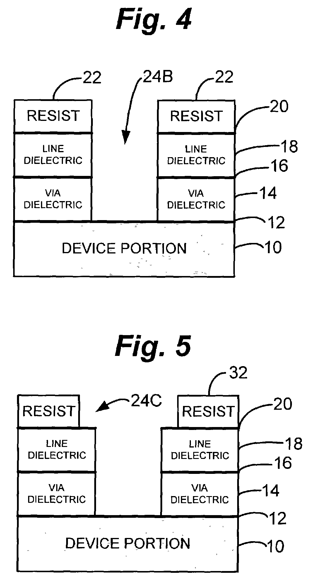
[0031]In FIG. 1, a device layer 10 is formed, which may be a simple silicon substrate and first-level metal, for example. The device layer 10 may nonetheless also include multiple levels of metal, transistors, capacitors, or other devices, including previously manufactured integrated air gap structures built according to the method of the present invention. Thus, device layer 10 is meant to represent that portion of the previously formed integrated circuit device on which the air gap structure is to be built, but it is not limited to any particular form, structure or circuitry.

[0032]Similarly, as used herein, the terms “on” or “onto” or “above” when used in connection with various thin film layers are merely intended to denote a physical spatial relationship, and not necessarily a direct physical or...

second embodiment

[0074]Referring generally now to FIGS. 14-24, a method for forming an integrated circuit device having at least one air gap structure is shown for a conventional metal interconnect structure of the type having aluminum alloy metal interconnect layers and tungsten metal plugs. Except where otherwise noted, like numerals are intended to represent like structures and materials already identified in connection with FIGS. 1-13.

[0075]In FIG. 14, a device layer 10 is formed as before.

[0076]A contact / via dielectric layer 14 is formed on device layer 10. As before, dielectric layer 14 is ideally silicon dioxide but can also be USG, FSG, PSG, BPSG, or the like and is deposited to a thickness of about 1000 to 10000 Angstroms. It will be understood, of course, that layer 14 may be comprised of a combination of layers, and formed in more than one processing step, but for purposes of the present discussion, it will be referred to as a single layer.

[0077]In FIG. 15, a photoresist layer 22 is forme...

third embodiment

[0090]Referring generally now to FIGS. 25-33, a third embodiment of a method for forming an integrated circuit device having at least an air gap structure is shown for a conventional metal interconnect structure of the type having aluminum alloy metal interconnect layers and aluminum alloy metal plugs. The primary difference to the second embodiment is in the use of a different type of a barrier metal layer for the interlayer plugs.

[0091]In FIG. 25, a contact / via dielectric layer 14 is formed on device layer 10 as before.

[0092]In FIG. 26, a photoresist layer 22 is formed and patterned on dielectric layer 14 as before to form a pattern of openings 86A.

[0093]In FIG. 27, openings 86B are etched into contact / via dielectric layer 14 as before.

[0094]In FIG. 28, resist layer 22 is stripped and an aluminum barrier layer 94 (such as Ti / TiN, Ta, TaN or Aluminum oxide) is deposited on the surface of dielectric layer 82 and in openings 86. Again, these are merely examples of those known at this...


PUM


Abstract

An air gap structure and formation method for substantially reducing capacitance in a dual damascene based interconnect structure is disclosed. The air gap extends above, and may also additionally extend below, the damascene interconnects desired to be isolated thus minimizing fringing fields between the lines. Multiple levels of the integrated air gap structure can be fabricated to accommodate multiple metal levels.

Description

CROSS REFERENCE TO RELATED APPLICATIONS[0001]The present application is related to the following applications all filed on this same date herewith:[0002]Air Gap Structure And Formation Method For Reducing Undesired Capacitive Coupling Between Interconnects In An Integrated Circuit Device, Ser. No. 10 / 295,062;[0003]Air Gap for Tungsten / Aluminum Plug applications Ser. No. 11 / 295,080;[0004]The aforementioned are hereby incorporated by reference as if fully set forth herein.FIELD OF THE INVENTION[0005]The present invention relates, in general, to the field of integrated circuit (“IC”) device structures and methods of forming the same. More particularly, the present invention relates to an air gap structure and formation method for use in a damascene interconnect in an integrated circuit device.BACKGROUND OF THE INVENTION[0006]As integrated circuit transistor densities increase, and feature sizes shrink, capacitive coupling between adjacent interconnects, metal lines or other elements al...

Claims


Application Information

Patent Timeline
Patent Type & Authority Patents(United States)
IPC IPC(8): H01L21/764H01L21/768H01L23/522
CPCH01L21/76807H01L21/76813H01L21/7682H01L23/5222H01L2924/0002H01L21/76885H01L23/53295H01L2924/00
Inventor LUR, WATERLEE, DAVIDWANG, KUANG-CHIHYANG, MING-SHENG
Owner UNITED MICROELECTRONICS CORP
Why Eureka
Try Eureka