Silicon tolerance specification using shapes as design intent markers

a technology of design intent and silicon, applied in the direction of instrumentation, program control, cad circuit design, etc., can solve the problems of not being aware of which shapes are critical and which are non-critical, and the amount of opc features inserted could be dramatically reduced, so as to improve yield and/or cost

Active Publication Date: 2008-11-25
SYNOPSYS INC
View PDF7 Cites 201 Cited by
  • Summary
  • Abstract
  • Description
  • Claims
  • Application Information

AI Technical Summary

Benefits of technology

[0013]During manufacturing, the manufacturing tools use shapes and / or regions identified by the mapping tools, to automatically change silicon tolerance from default, for example based on a predetermined rule and / or a predetermined correspondence between tolerances and attribute values (e.g. obtained by experimentation). For example, in regions that are automatically selected as described above, one or more silicon tolerances are not relaxed during manufacturing of shapes contained therein, although tolerances are relaxed everywhere else to improve yield and / or cost and / or turn-around-time and / or size of mask data etc. Different levels of (or different kinds of) resolution enhancements may be performed (or not performed) on selected shapes, depending on different levels of aggressiveness at which geometries are to be maintained, which in turn depends on a circuit designer's manual indication of limits and / or ranges and / or criticality of design attributes.

Problems solved by technology

However, traditional manufacturing tools (such as mask synthesis, mask writer, mask inspection, wafer inspection and mask data preparation tools) are not aware of which shapes are critical and which are non-critical.
This article quotes Graham Bell, director of marketing for Nassda Corp as stating “The RTL to GDSII flow really means that when you are at the RTL stage, you have a sense of what your GDSII is,” On the other hand, with design intent with the RTL to GDSII flow, the whole emphasis is on physical implementation, and that doesn't address the functional verification.
In a second example, if the tool that inserted OPC was aware of the actual timing requirements of the nets on which it was working, the amount of OPC features inserted could be dramatically reduced, with a very significant impact on mask cost.

Method used


Image

  • Silicon tolerance specification using shapes as design intent markers
  • Silicon tolerance specification using shapes as design intent markers
  • Silicon tolerance specification using shapes as design intent markers

Examples


Embodiment Construction

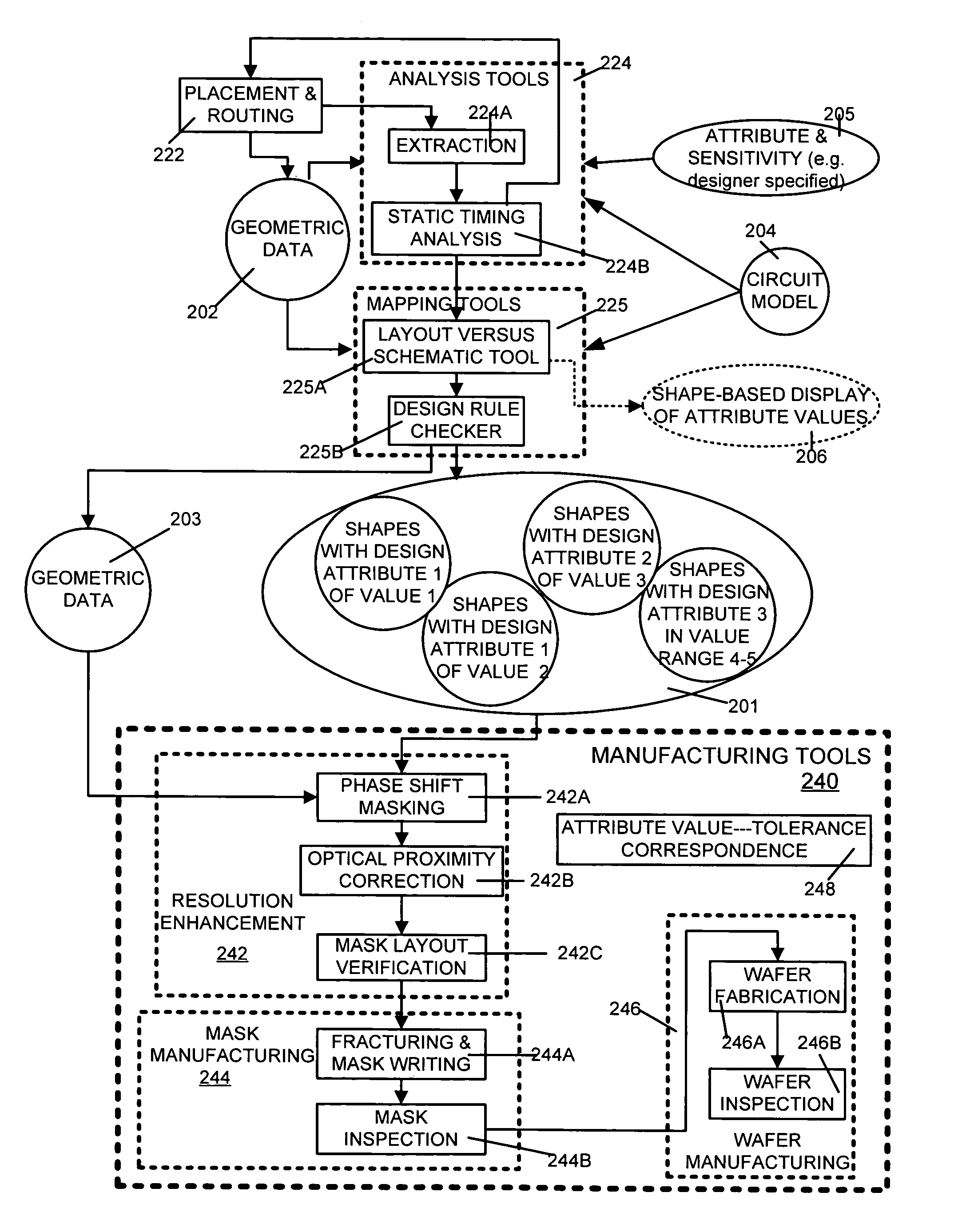
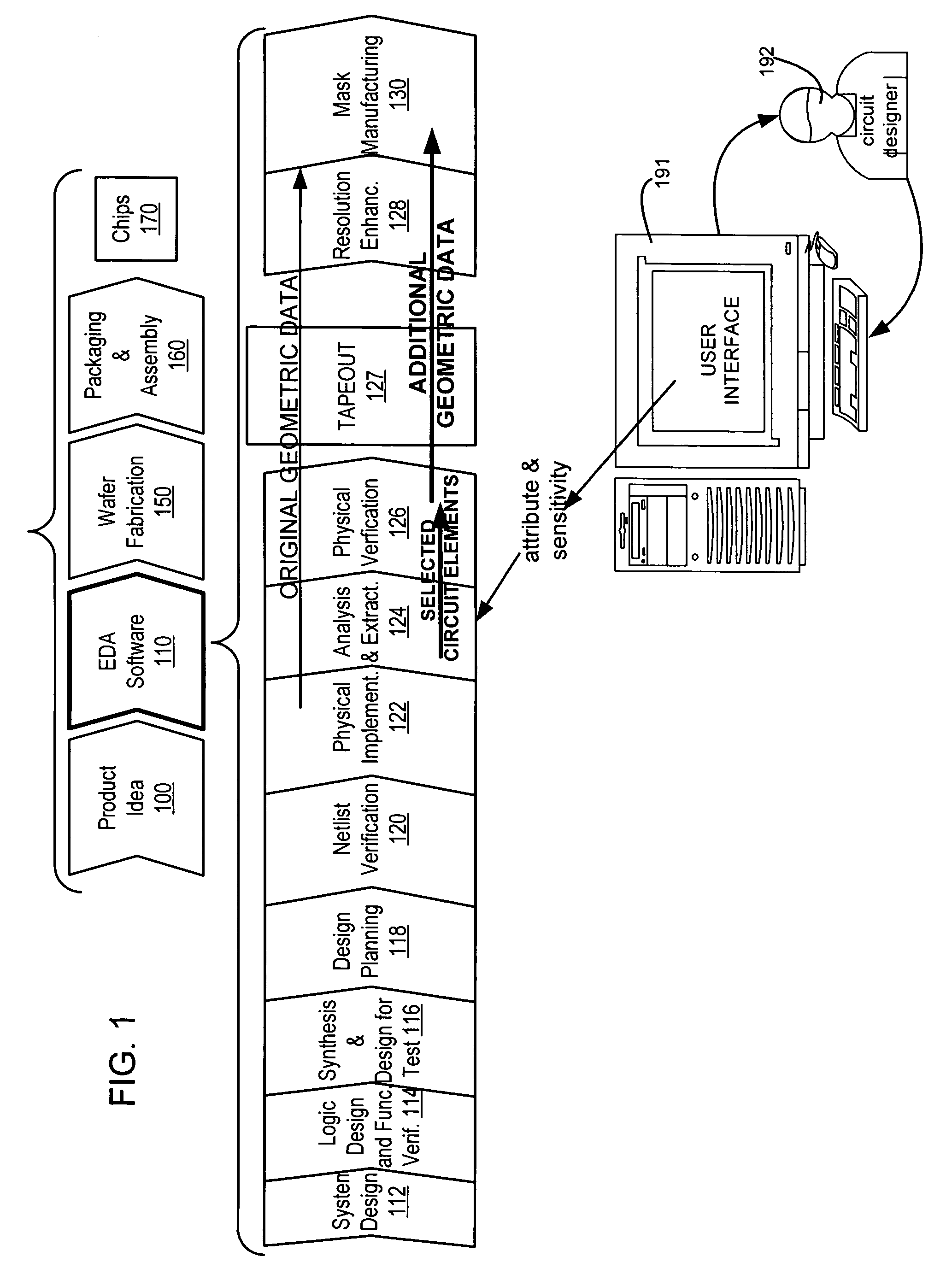
[0026]At a high level, a process for creating integrated circuit chips starts with a product idea 100 (FIG. 1) and is realized in a EDA software design process 110. After the EDA software design process, a fabrication stage 150 and packaging and assembly processes 160 occur resulting, ultimately, in finished chips (result 170). EDA software design process 110 is actually composed of a number of stages 112-130, shown in linear fashion for simplicity in FIG. 1. In an actual ASIC design process, the particular design might have to go back through steps until certain tests are passed. Similarly, in any actual design process, these steps may occur in different orders and combinations. This description is therefore provided by way of context and general explanation rather than as a specific, or recommended, design flow for a particular ASIC. A brief description of the components of the EDA software design process 110 is provided below, in the next few paragraphs.

[0027]System design (stage...


PUM


Abstract

Design-specific attributes of a circuit (such as timing, power, electro-migration, and signal integrity) are used to automatically identify one or more regions of one or more layers in a layout of the circuit. The automatically identified regions may be provided to a manufacturing tool in GDSII by use of overlapping shapes in, or alternatively by moving existing shapes to, a different layer / datatype pair. For example, information about the automatically identified regions may be stored using a conventional datatype (e.g. value 0) with a new layer, or alternatively using a conventional layer (e.g. metal 3) with a new datatype (e.g. value 1), depending on the embodiment. The automatically identified regions contain cells and / or features (e.g. groups of shapes and / or individual shapes) whose tolerance in silicon (to be fabricated) is automatically changed from default, based on the design-specific attribute(s) and sensitivity thereto, expressed as design intent by a circuit designer.

Description

BACKGROUND[0001]1. Field of the Invention[0002]The invention relates to design of semiconductor chips. More specifically, the invention relates to a method and an apparatus for using the effect of shapes on design-specific attributes to indirectly specify tolerances to be applied in manufacturing semiconductor devices via design intent.[0003]2. Related Art[0004]Traditionally, design data provided to manufacturing to specify the silicon structures comprising an integrated circuit, e.g. in the form of GDSII, contained geometrical information describing a single specific rendering of the silicon layout. Yield was achieved by producing parts very close to the specified geometries. Such a traditional process doesn't account for the fact that most features in any layout are not timing critical, and for such features a certain level of process variation may be tolerable. Less-aggressive optical proximity correction (OPC) for such non-critical features can lower costs. However, traditional ...

Claims


Application Information

Patent Timeline
Patent Type & Authority Patents(United States)
IPC IPC(8): G06F17/50
CPCG06F17/5036G06F17/5068G06F30/367G06F30/39
Inventor COTE, MICHELRIEGER, MICHAELHURAT, PHILIPPELUGG, ROBERTMAYHEW, JEFF
Owner SYNOPSYS INC
Why Eureka
Try Eureka