Chemically amplified resist composition, process for manufacturing semiconductor device and patterning process

a semiconductor device and composition technology, applied in the field of chemical amplified resist composition, can solve the problems of less reliable semiconductor devices, inability to shape the interlayer insulating film into the desired shape, so as to prevent the deterioration of resist sensitivity, reduce the fluctuation of patterning resolution, and improve the effect of processing properties

Active Publication Date: 2009-01-20
RENESAS ELECTRONICS CORP
View PDF16 Cites 31 Cited by
  • Summary
  • Abstract
  • Description
  • Claims
  • Application Information

AI Technical Summary

Benefits of technology

[0035]In this invention, the salt may include a basic compound which can be used as a quencher. Herein, a basic compound which can be used as a quencher means a compound which inhibits diffusion of an acid generated from a photoacid generator in a resist film; for example, a nitrogen-containing basic compound. Such a basic compound may be used to minimize fluctuation of resolution in patterning and to form reliably a desired pattern. In this invention, the salt may be an amine. Thus, deterioration in sensitivity in a resist can be more reliably prevented.
[0036]In this invention, a salt of an alkanolamine with a sulfonic acid can be used as the salt. The sulfonic acid preferably may include benzenesulfonic acid, alkylsulfonic acid, camphorsulfonic acid and these substituted derivatives. Substituted derivatives include mono- and poly-substituted derivatives, those substituted with an organic group such as alkyl and alkoxy, and those substituted with a halogen such as fluorine, as well as those substituted with a fluoroalkyl. When introducing a substituent such as alkyl and alkoxy, it is preferable to select the proper carbon number. For example, a substituent with up to three carbon atoms may give a product having good handling properties.
[0037]A salt constituted with the above combination may be used to further reliably exert buffering action and thus to further reliably prevent sensitivity deterioration in lithography.
[0038]In this invention, an alkali solubility of the base resin may be varied by the action of the acid. In a negative resist, a generated acid causes a crosslinking reaction to form a site with a reduced solubility in a developer. In a positive resist, a generated acid dissociates a protective group in a resin to improve solubility. Thus, for example in a chemically amplified resist composition of this invention, the base resin may have an alkali-soluble group protected with a dissolution-inhibiting group and the dissolution-inhibiting group may be dissociated by the action of the acid to give an alkali-soluble resin. A resist composition according to this invention comprises a salt exhibiting buffer effect, so that when using such a base resin, fluctuation of alkali solubility due to variation in exposure can be prevented.
[0039]In a process for manufacturing a semiconductor device of this invention, the step of removing a first resist film may comprise removing a part of the first resist film using an amine stripper. In the manufacturing process of this invention, a second resist film comprising a salt exhibiting buffer effect is formed. Thus, deterioration in sensitivity can be reliably prevented when an amine component present in a stripper used for removing the first resist film remains in a film to be etched and permeates into the second resist film.
[0040]In a process for manufacturing a semiconductor device of this invention, the film to be etched may contain nitrogen. In a process for forming a pattern of this invention, the material to be etched may contain nitrogen. In a manufacturing process of this invention, a resist film comprising a salt exhibiting buffer effect is formed. Thus, deterioration in sensitivity can be reliably prevented when a nitrogen-containing basic compound derived from a film to be etched or an etching agent permeates into a resist film.

Problems solved by technology

If resist poisoning occurs, an interlayer insulating film cannot be processed into a desired shape.
Furthermore, when directly forming an interconnection, interconnection-defects such as stress-migration and electro-migration may occur, leading to a less reliable semiconductor device.
However, when adding a quencher to a resist composition, it is effective for preventing resist poisoning during resist patterning, but it may lead to deteriorate in resist sensitivity.
A resist with excessively lower sensitivity may reduce a throughput in an exposure process and thus may sometimes lead to significantly deteriorated mass productivity.
Thus, when adding a sufficient amount of the quencher to completely prevent poisoning, an exposure time frequently exceed a permissible limit.
Furthermore, in a lithography process with a lower throughput such as EB direct-drawing lithography, it is difficult to increase the amount of the quencher for preventing resist poisoning.
Thus, the process cannot be sometimes employed due to resist poisoning.
Specifically, it has been found that an amine or its analogue is formed in an interlayer insulating film formed on a semiconductor substrate and the compound is subjected to neutralization with an acid catalyst in a chemically amplified resist, leading to deteriorated sensitivity of a resist.

Method used


Image

  • Chemically amplified resist composition, process for manufacturing semiconductor device and patterning process
  • Chemically amplified resist composition, process for manufacturing semiconductor device and patterning process
  • Chemically amplified resist composition, process for manufacturing semiconductor device and patterning process

Examples


embodiment 1

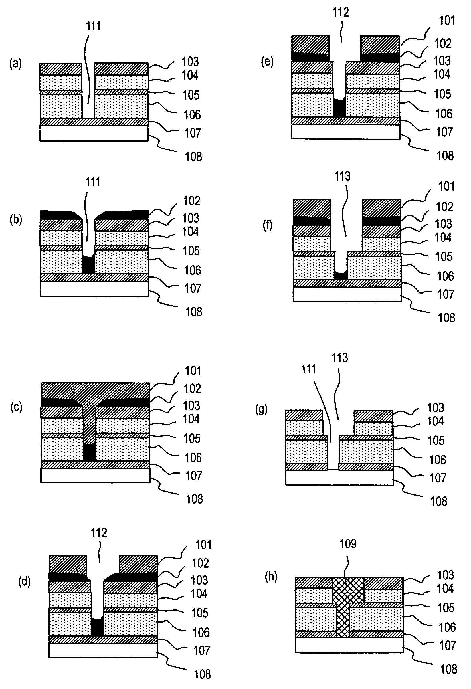
[0114]This embodiment illustrates a dual damascene process employing a via-first method, using a chemically amplified resist composition. FIG. 1 is cross-sectional views showing a manufacturing process for a semiconductor device according to this embodiment.

[0115]First, on a lower interconnection layer 108 are sequentially deposited a first etching stopper film 107, a first interlayer insulating film 106, a second etching stopper film 105, a second interlayer insulating film 104 and a third interlayer insulating film 103. Then, using well-known lithography and etching technique, a via-hole 111 is formed in the third interlayer insulating film 103, the second interlayer insulating film 104, the second etching stopper film 105 and the first interlayer insulating film 106 (FIG. 1(a)).

[0116]Then, an anti-reflection film 102 is formed on the third interlayer insulating film 103 and the first etching stopper film 107, during which the via-hole 111 is partly or totally buried with the anti...

embodiment 2

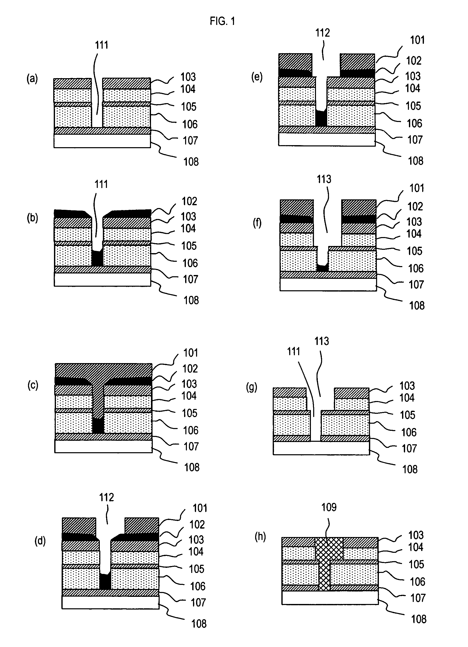
[0126]The interconnection structure in FIG. 1(h) may be also manufactured by a so-called trench-first method among dual damascene processes. There will be described a copper interconnection structure manufactured by a trench-first method with reference to FIG. 2. In this embodiment, similar components to those in Embodiment 1 are identified with the same symbols without any description as appropriate.

[0127]As described in Embodiment 1, on a lower interconnection layer 108 are sequentially deposited a first etching stopper film 107, a first interlayer insulating film 106, a second etching stopper film 105, a second interlayer insulating film 104 and a third interlayer insulating film 103. Then, using well-known lithography and etching technique, an interconnection trench 113 is formed in the third interlayer insulating film 103 and the second interlayer insulating film 104 (FIG. 2(a)).

[0128]Then, an anti-reflection film 102 is formed on the third interlayer insulating film 103 and th...

embodiment 3

[0133]The resist composition used in Embodiment 1 or 2 can be applied to a via-first dual damascene process using a three-layer resist method. There will be described this process with reference to FIG. 3.

[0134]First, on a lower interconnection layer 108 are sequentially deposited a first etching stopper film 107 and an interlayer insulating film 115. Then, using well-known lithography and etching technique, a via-hole 111 is formed in the interlayer insulating film 115 (FIG. 3(a)).

[0135]Then, an anti-reflection film (not shown) is formed on the interlayer insulating film 115 and the first etching stopper film 107, during which the via-hole 111 is partly or totally buried with the anti-reflection film. Then, on the anti-reflection film is applied a three-layer resist film consisting of a first resist film 116, a second resist film 117 and a third resist film 118, in which the first resist film 116 comprises the resist composition described above. Then, in the third resist film 118 i...


PUM

PropertyMeasurementUnit
specific dielectric constantaaaaaaaaaa
wavelengthaaaaaaaaaa

Abstract

An objective of this invention is to prevent resist poisoning and sensitivity deterioration in a chemically amplified resist. The chemically amplified resist comprises a base resin, a photoacid generator and a salt exhibiting buffer effect in the base resin.

Description

BACKGROUND OF THE INVENTION[0001]1. Field of the Invention[0002]This invention relates to a chemically amplified resist composition, a process for manufacturing a semiconductor device and a patterning process.[0003]2. Description of the Prior Art[0004]As a device has become more compact and more accelerated, lithography using a short-wavelength light source has been employed because of improving resolution. In addition, there has been used a chemically amplified resist as a resist material.[0005]Furthermore, the needs for size reduction and acceleration in a semiconductor device require using, besides a copper (Cu) interconnection, a so-called low dielectric constant material. A copper interconnection is generally formed by a damascene process in which a trench for an interconnection is formed on an insulating film between interconnections, the trench is filled with copper and then excessive copper in an unwanted area outside the interconnection trench is removed by chemical mechani...

Claims


Application Information

Patent Timeline
Patent Type & Authority Patents(United States)
IPC IPC(8): G03F7/00G03F7/004G03F7/038G03F7/039G03F7/11G03F7/40H01L21/027H01L21/768
CPCG03F7/0382G03F7/0392H01L21/76807H01L21/76808
Inventor NAGAHARA, SEIJIHIROI, MASAYUKI
Owner RENESAS ELECTRONICS CORP
Why Eureka
Try Eureka