

Manufacturing method of semiconductor device
a manufacturing method and semiconductor technology, applied in the direction of semiconductor devices, electrical appliances, basic electric elements, etc., can solve the problems of increased cost, difficult to reuse a substrate, and affect the property of transistors, and achieve the effect of low cost and high reliability
- Summary
- Abstract
- Description
- Claims
- Application Information
AI Technical Summary
Benefits of technology
Problems solved by technology
Method used
Image

Examples
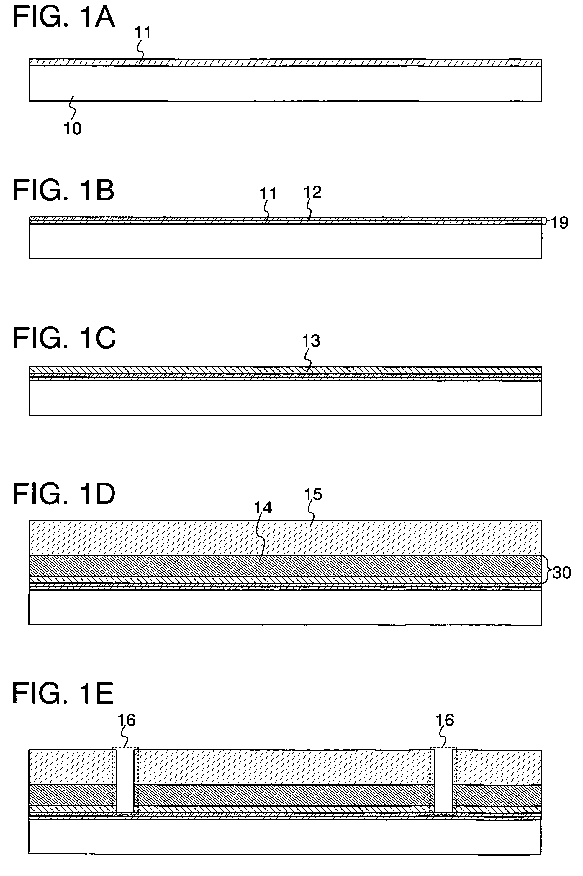
embodiment mode 1
[0034]In this embodiment mode, one example of a manufacturing method of a semiconductor device of the invention is described with reference to the drawings.
[0035]First, a metal film 11 is formed on a surface of a substrate 10 (FIG. 1A). The metal film 11 may be formed by a single layer or a plurality of layers stacked. For example, a tungsten (W) film is formed by sputtering. It is to be noted that an insulating film may be provided on the substrate 10 before the metal film 11 is formed. In particular, it is preferable to provide an insulating film between the substrate 10 and the metal film 11 when the contamination from the substrate may occur.
[0036]Next, plasma treatment is applied to the metal film 11 in an atmosphere of oxygen to form a metal oxide film 12 on a surface of the metal film 11 (FIG. 1B). The metal oxide film 12 is formed by using a metal oxide of a metal for the metal film 11. For example, when a tungsten film is used as the metal film 11, a tungsten oxide film is ...
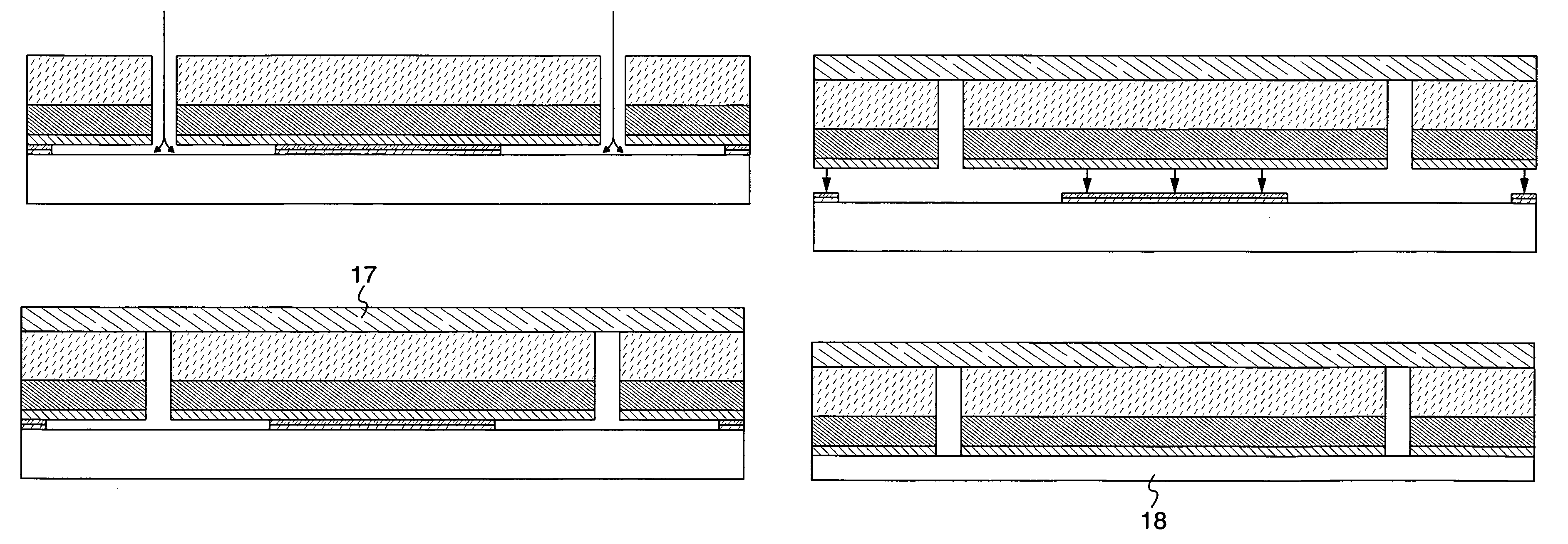
embodiment mode 2
[0059]In this embodiment mode, a manufacturing method of a semiconductor device different from the above embodiment mode is described with reference to the drawings.
[0060]First, the metal film 11 is formed on a surface of the substrate 10 (FIG. 4A). The metal film 11 may be formed by a single layer or a plurality of layers stacked. For example, a tungsten (W) film is formed by sputtering. It is to be noted that an insulating film may be provided on the substrate 10 before the metal film 11 is formed. In particular, it is preferable to provide an insulating film between the substrate 10 and the metal film 11 when the contamination from the substrate may occur.
[0061]Then, in this embodiment mode, heat treatment using an RTA or an annealing furnace is performed to oxidize the metal film 11 so that a metal oxide film 22 is formed on a surface of the metal film 11. Described here is a case where the heat treatment is performed using an RTA (FIG. 4B). FIG. 4B shows an apparatus for heatin...
embodiment mode 3
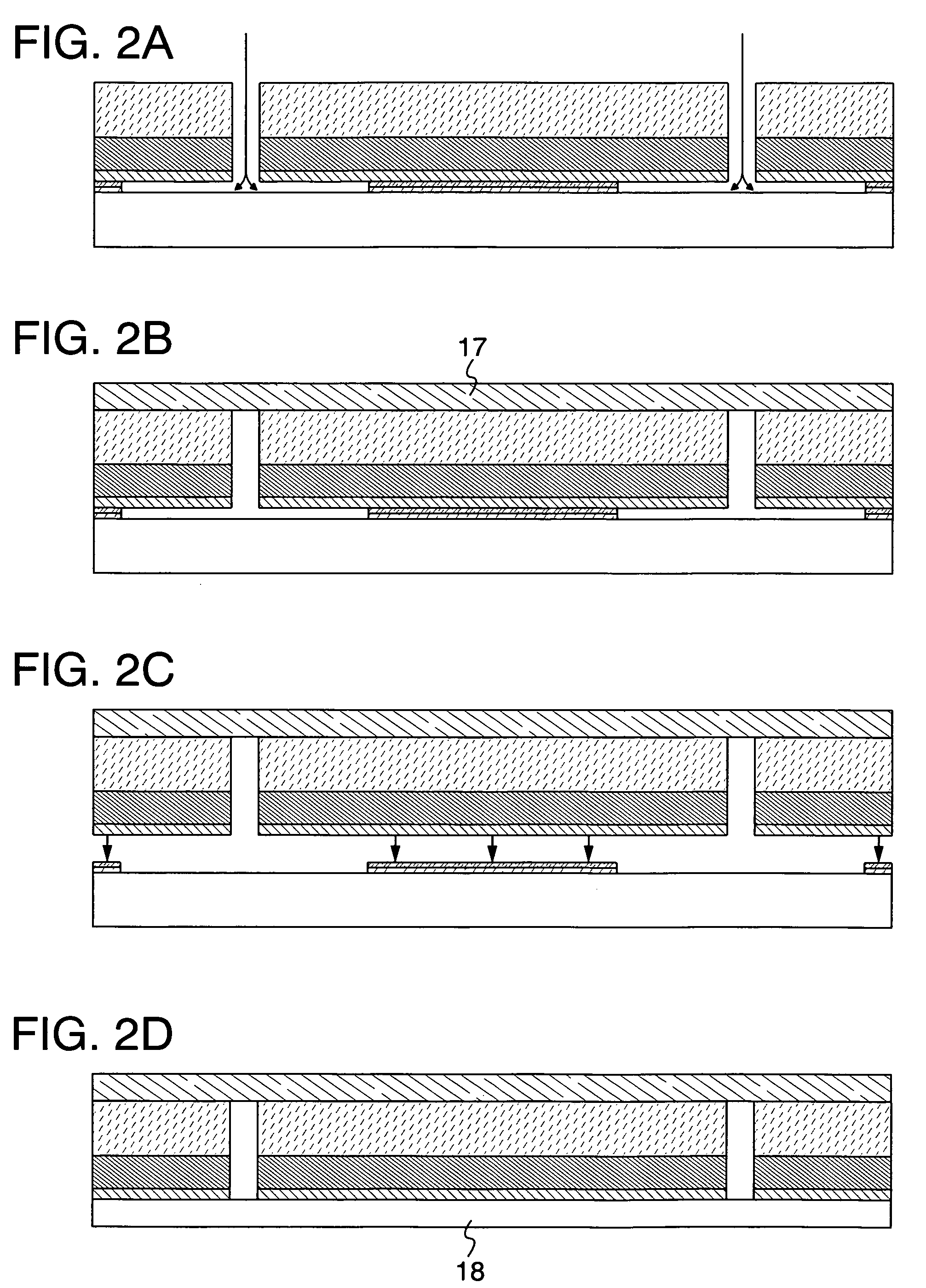
[0066]In this embodiment mode, a manufacturing method of a semiconductor device different from the above embodiment modes is described with reference to the drawings.
[0067]First, a metal oxide film 31 is formed on a surface of the substrate 10 by sputtering in an atmosphere of oxygen (FIG. 5A). For example, the sputtering is performed using tungsten as a target in an atmosphere of argon and oxygen to form a tungsten oxide film (WOx) on the substrate 10. Other than tungsten, the metal oxide film 31 may be formed in a single layer or a multilayer structure by a film using an element selected from molybdenum (Mo), titanium (Ti), tantalum (Ta), niobium (Nb), nickel (Ni), cobalt (Co), zirconium (Zr), zinc (Zn), ruthenium (Ru), rhodium (Rh), lead (Pb), osmium (Os), iridium (Ir), and silicon (Si), an alloy material or a compound material containing the above-described element as its main component.
[0068]Next, the insulating film 13 is formed on the metal oxide film 31 (FIG. 5B). The insula...
PUM
| Property | Measurement | Unit |
|---|---|---|
| temperature | aaaaa | aaaaa |
| thickness | aaaaa | aaaaa |
| thickness | aaaaa | aaaaa |
Abstract
Description
Claims
Application Information