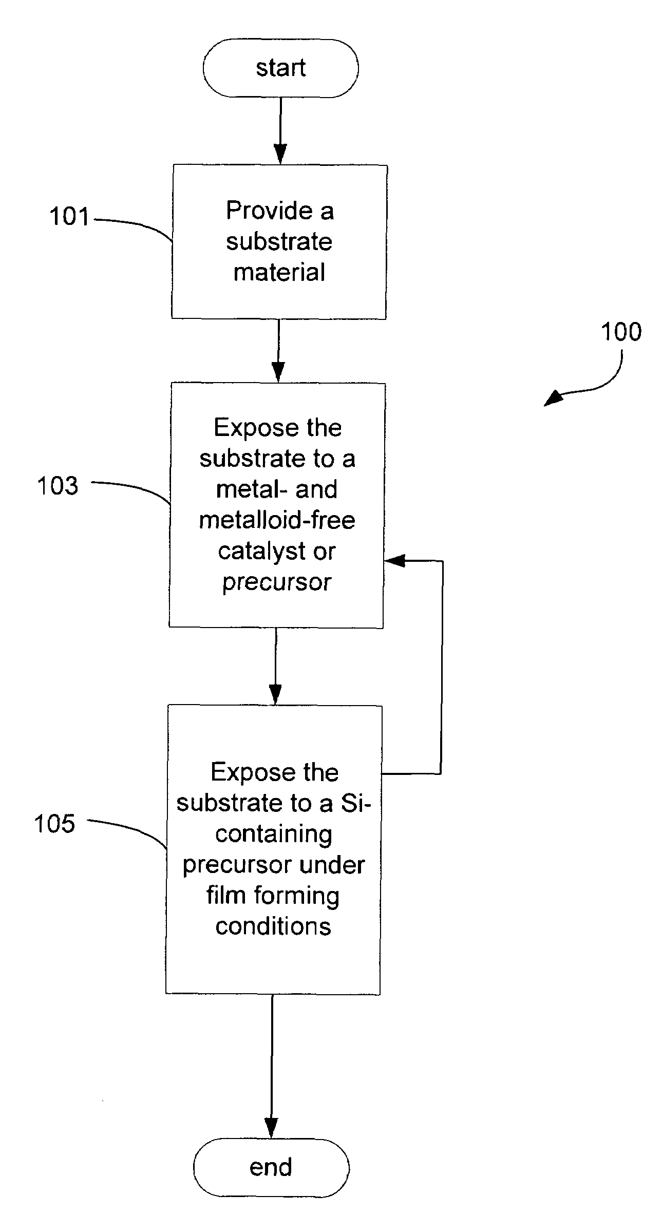
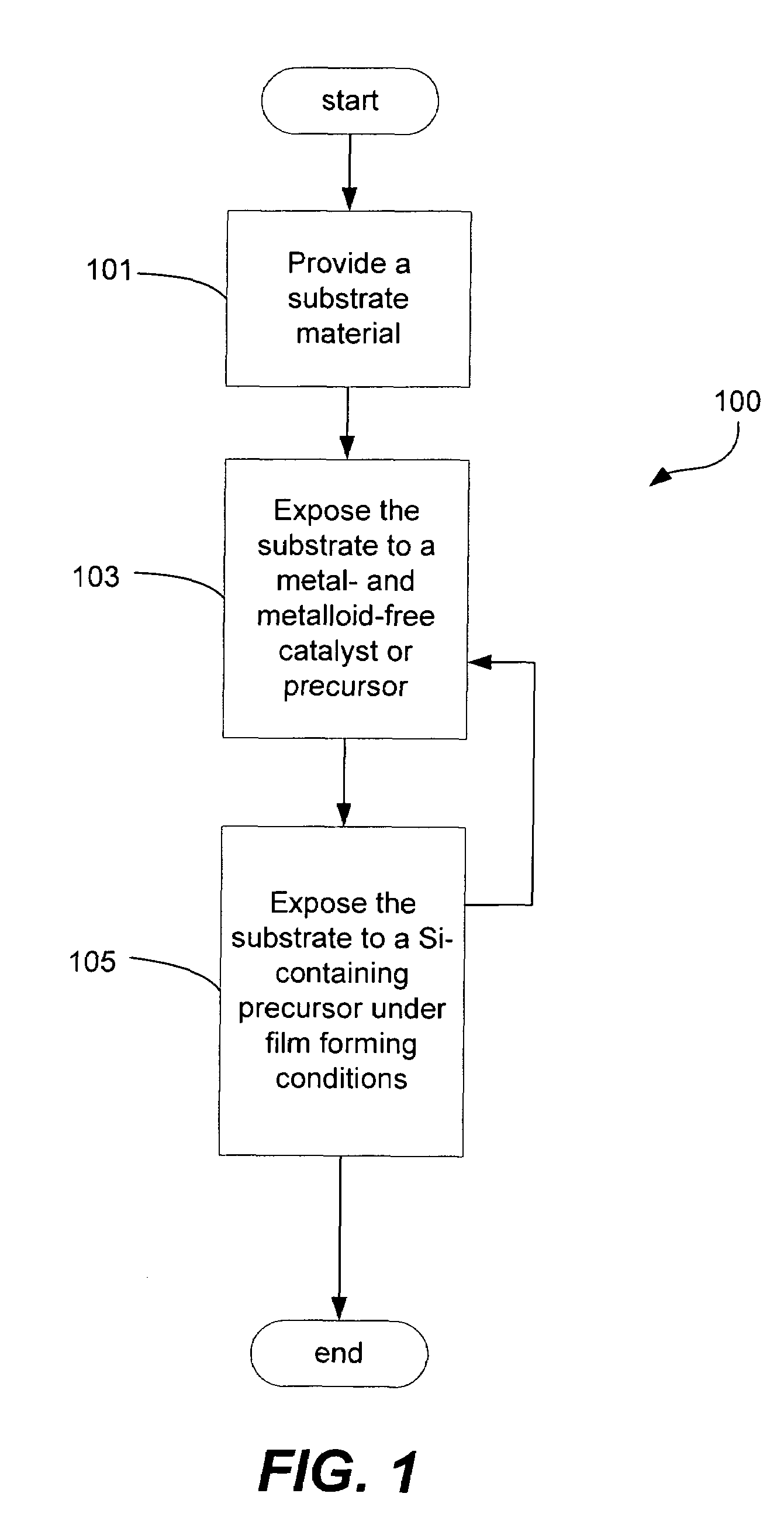
Metal-free catalysts for pulsed deposition layer process for conformal silica laminates
a conformal silica laminate, metal-free technology, applied in the direction of basic electric elements, semiconductor/solid-state device manufacturing, electric apparatus, etc., can solve the problems of void-free filling of high aspect ratio (ar) spaces (ar>3.0:1), shrinking dimensions, and increasing budgets, so as to improve performance characteristics
- Summary
- Abstract
- Description
- Claims
- Application Information
AI Technical Summary
Benefits of technology
Problems solved by technology
Method used
Image

Examples
examples
[0042]The following example provides details relating to performance advantages of the present invention. It should be understood the following is representative only, and that the invention is not limited by the detail set forth in this example.
[0043]The feasibility of the method was demonstrated using phosphoric acid (H3PO4) as a catalyst for a metal and metalloid-free pulsed layer deposition (PDL) process for dielectric film deposition in accordance with the present invention. Si substrates were exposed to the 7.1M phosphoric acid for 5 seconds and subsequently to TPOSL (tris t-pentoxy silanol) under conditions used for the deposition of PDL oxide (230° C., 20 Torr reactor pressure).
[0044]Film growth as a function of exposure cycles is shown in FIG. 3. The average growth rate is 334 Å / cycle. Baseline experiments showed no film growth without the presence of the acid, even after long exposure (8 hrs) to 20 Torr of TPOSL / N2 mixtures.
[0045]FIG. 4 shows the FTIR spectra of the deposi...
PUM
 Abstract
Description
Claims
Application Information