Semiconductor device and manufacturing method of the same

a technology of semiconductors and manufacturing methods, applied in semiconductor/solid-state device manufacturing, basic electric elements, electric devices, etc., can solve the problems of increasing the difficulty of tddb life, deteriorating tddb life, and extremely short life of tddb (time dependence on dielectric breakdown)

Active Publication Date: 2009-03-10
KOKUSA ELECTRIC CO LTD
View PDF13 Cites 24 Cited by
  • Summary
  • Abstract
  • Description
  • Claims
  • Application Information

AI Technical Summary

Benefits of technology

[0009]The present invention intends to provide a semiconductor device capable of improving the dielectric breakdown voltage between interconnections using copper as a main conductor layer, as well as a manufacturing method thereof.
[0040]The dielectric breakdown between interconnections can be improved, and capacitance between the interconnections can be decreased while taking a countermeasure for misalignment via hole.

Problems solved by technology

Use of copper for the interconnection material involves a problem that a TDDB (Time Dependence on Dielectric Breakdown) life is extremely shorter than that of other metal materials (for example, aluminum and tungsten).
In addition, while an insulative material of lower dielectric constant than that of silicon oxide has tended to be used as an insulative film between the interconnections with a view point that the interconnection pitch has become finer and the effective electric field intensity tends to be increased and in view of decrease in the interconnection capacitance in recent years, since the insulative film of low dielectric constant generally has low insulative dielectric breakdown voltage, securement for TDDB life has become difficult more and more.
Further, since the air gap is formed by inversely tapering the interconnection, electric fields are concentrated to the upper end of the interconnection to further deteriorate the TDDB life.
Further, JP-A No. 2001-85519 does not disclose at all the formation of a via hole to be connected with the interconnection.
However, countermeasure for the misaligned via hole is not taken into consideration at all in JP-A No. 2003-297918 and this results in a problem that misalignment with the interconnection occurs at the through hole position for forming the via hole by an exposure apparatus in a lithographic process and, in a case where an air gap is present below the through hole, a cleaning solution or Cu plating solution penetrates subsequently to result in failure of electric connection or increase of the capacitance.

Method used


Image

  • Semiconductor device and manufacturing method of the same
  • Semiconductor device and manufacturing method of the same
  • Semiconductor device and manufacturing method of the same

Examples


embodiment 1

[0084]At first, the cause for the degradation of the TDDB life between a buried interconnection using the copper as the main conductor layer described above by the present inventors is to be explained. The TDDB (Time Dependence on Dielectric Breakdown) life is a measure for objectively determining the time dependence of dielectric breakdown, which is a time (life) obtained by applying a relatively high voltage between electrodes under a measuring condition at a predetermined temperature (for example, 140° C.), preparing a graph by plotting a time from voltage application to dielectric breakdown relative to the applied electric field and extrapolating to an electric field intensity actually used (for example, 0.2 MV / cm) in view of the graph.

[0085]Degradation of the TDDB life is generally considered to be attributable to that copper applied to the interconnection material diffuses to the periphery, and lowers the dielectric breakdown voltage between interconnections. However, accordin...

embodiment 2

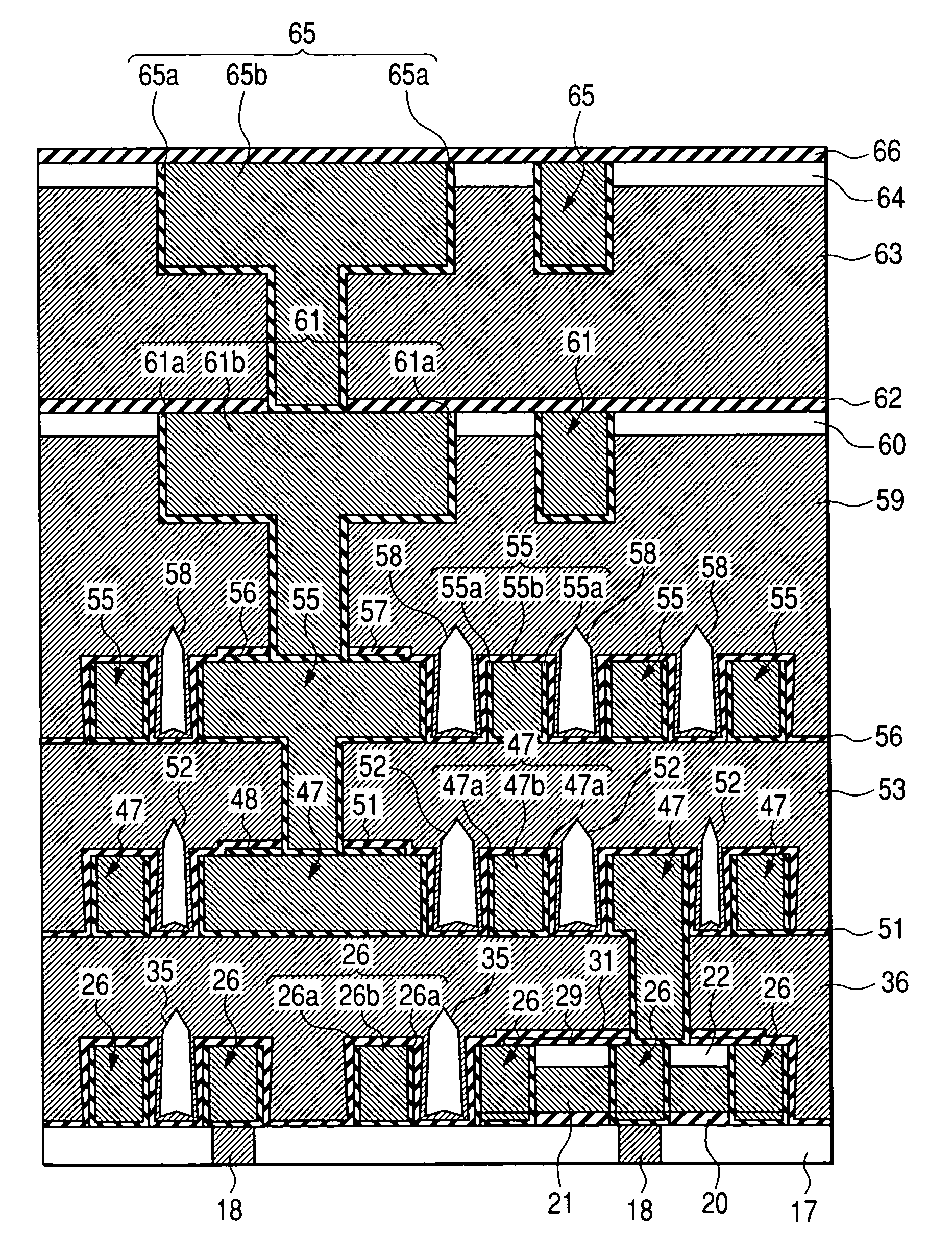
[0143]FIG. 31 is a cross sectional view for a main portion in the manufacturing step of a semiconductor device as other embodiment of the invention. The semiconductor device of this embodiment has a multi-layered interconnection structure having, in combination, a structure with an air gap being formed between adjacent interconnections and having an interconnection layer not connecting adjacent interconnections with a CMP surface and having a reservoir as in the second layer interconnection layer 26 and the third layer interconnection 47 of the embodiment 1 and an interconnection layer formed by using a general embedding interconnection technique. In FIG. 31, since the steps up to the formation of the insulative film 60 above the fourth layer interconnection 55 are substantially identical with the manufacturing steps of FIG. 4 to FIG. 10 and FIG. 18 to FIG. 30 of the embodiment 1, explanation therefor is omitted and only the subsequent manufacturing steps are to be described herein....

embodiment 3

[0147]FIG. 32 is a cross sectional view for a main portion in the manufacturing step of a semiconductor device as other embodiment of the invention succeeding to FIG. 3. Also in FIG. 32, those portions corresponding to the structure below the insulative film 17 in FIG. 3 are not illustrated in the drawing.

[0148]This embodiment shows an air gap-interconnection in a case of forming an interconnection layer from a conductive film typically represented by an aluminum (Al) interconnection by a dry etching method.

[0149]At first in this embodiment, as shown in FIG. 32, a conductive film 70 is formed over an insulative film 17 in which a through hole 18 is buried by a sputtering method or a CVD method. The conductive film 70 referred to herein is not restricted only to aluminum but may be changed variously. For example, it may also be a single film formed, for example, of aluminum (Al) or aluminum alloy, or a laminate metal film in which a metal film such as of titanium (Ti) or titanium nit...


PUM


Abstract

In a semiconductor device, capacitance between copper interconnections is decreased and the insulation breakdown is improved simultaneously, and a countermeasure is taken for misalignment via by a manufacturing method including the steps of forming an interconnection containing copper as a main ingredient in an insulative film above a substrate, forming insulative films and a barrier insulative film for a reservoir pattern, forming an insulative film capable of suppressing or preventing copper from diffusing on the upper surface and on the lateral surface of the interconnection and above the insulative film and the insulative film, forming insulative films of low dielectric constant, in which the insulative film is formed such that the deposition rate above the opposing lateral surfaces of the interconnections is larger than the deposition rate therebelow to form an air gap between the adjacent interconnections and, finally, planarizing the insulative film by interlayer CMP.

Description

CLAIM OF PRIORITY[0001]The present application claims priority from Japanese application JP 2005-167676 filed on Jun. 8, 2005, the content of which is hereby incorporated by reference into this application.FIELD OF THE INVENTION[0002]The present invention concerns a semiconductor device and a manufacturing technique thereof and, particularly, it relates to a technique effective for application to a semiconductor device having an interconnection containing a main conductor film comprising copper as a main ingredient.BACKGROUND OF THE INVENTION[0003]A buried interconnection structure is formed by burying an interconnection material in an interconnection opening such as an interconnection trench or hole formed in an insulative film by an interconnection forming technique referred to as a damascene technique (single-damascene) technique and a dual damascene technique. However, in a case of using copper (Cu) as a main material for the interconnection, since copper tends to be diffused mo...

Claims


Application Information

Patent Timeline
Patent Type & Authority Patents(United States)
IPC IPC(8): H01L21/311
CPCH01L21/76811H01L21/7682H01L21/76832H01L21/76834H01L21/76843
Inventor NOGUCHI, JUNJIMATSUMOTO, TAKASHIOSHIMA, TAKAYUKIONOZUKA, TOSHIHIKO
Owner KOKUSA ELECTRIC CO LTD
Why Eureka
Try Eureka