Electronic device package with an integrated evaporator

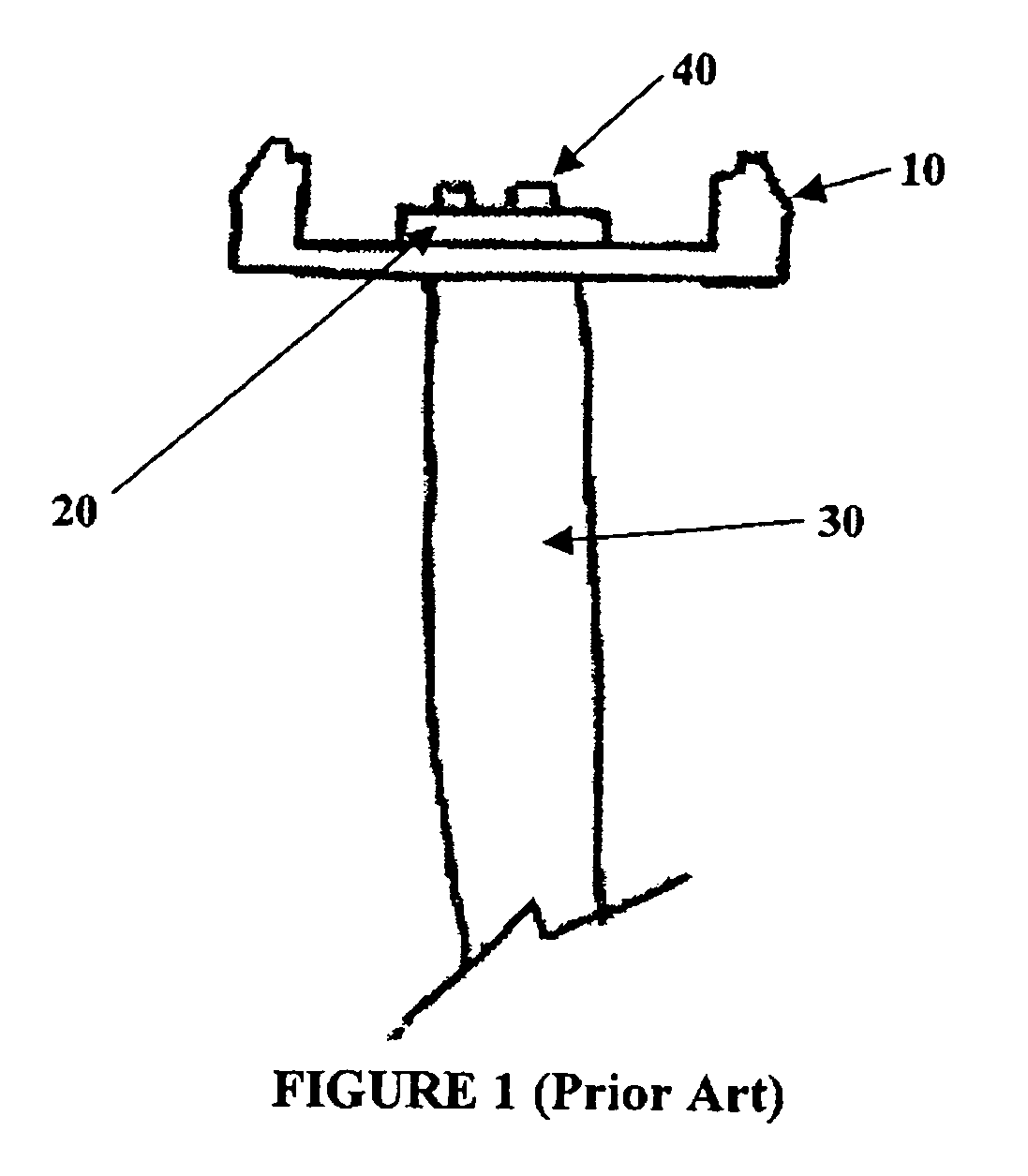
a technology of electronic devices and evaporators, applied in the direction of power cables, cables, semiconductor/solid-state device details, etc., can solve the problems of undesirable thermal resistance between the packages, failure of the electronic device, and the failure of the semiconductor devi

Active Publication Date: 2009-03-17
SIGNIFY HLDG BV
View PDF106 Cites 33 Cited by
  • Summary
  • Abstract
  • Description
  • Claims
  • Application Information

AI Technical Summary

Problems solved by technology

Typically, an electronic device for example, a semiconductor device, can fail when its junction temperature exceeds a certain threshold.
Generally, this technique provides an adequate but not optimal thermal interface to move and spread the heat generated by the electronic devices.
A downfall of current thermal solutions is that there is an undesirable thermal resistance that exists between the package and the thermal management system, for example a heat pipe.
This fact can result in an increase in the junction temperature of the semiconductor material or electronic devices, thereby resulting in reduced performance and a possible shorter lifetime thereof.
This package design has to conduct heat from the light-emitting diodes 40 to the heat pipe 30, however, minute changes in manufacturing or assembly tolerances can compromise heat transfer across the interfaces between the light-emitting diodes, the substrate, the carrier or housing, and the heat pipe.
This multi-chip module design includes a number of speciality requirements, including the creation of cavities within and along the length of the substrate, wherein it may not be possible to manufacture this requirement during standard electronic device package manufacturing.
Therefore the size of the heat pipe would be directly impacted by standard package manufacturing machinery, thereby potentially limiting the effectiveness of the heat extraction capability of the heat pipe.

Method used


Image

  • Electronic device package with an integrated evaporator
  • Electronic device package with an integrated evaporator
  • Electronic device package with an integrated evaporator

Examples


Embodiment Construction

Definitions

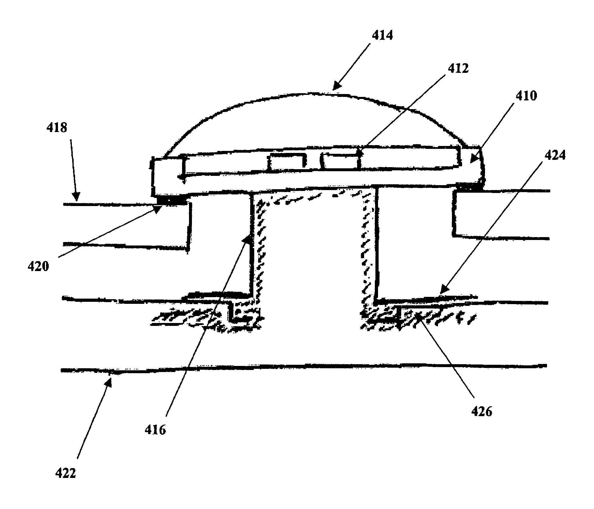
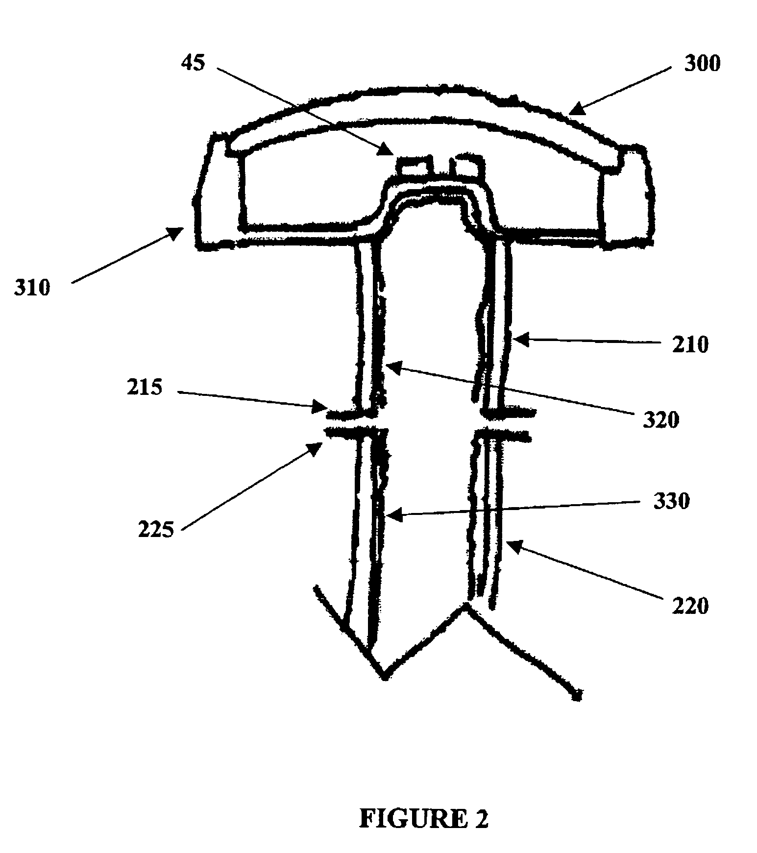
[0021]The term “electronic device” is used to define any device wherein its level of operation depends on the current being supplied or the voltage being applied thereto. An electronic device can be a light emitting element, electronics, semiconductor chip, motor or any other device requiring electrical current or voltage regulation as would be readily understood by a worker skilled in the art.

[0022]The term “light-emitting element” is used to define any device that emits radiation in any region or combination of regions of the electromagnetic spectrum for example, the visible region, infrared and / or ultraviolet region, when activated by applying a potential difference across it or passing a current through it, for example. Therefore a light-emitting element can have monochromatic, quasi-monochromatic, polychromatic or broadband spectral emission characteristics. Examples of light-emitting elements include semiconductor, organic, or polymer / polymeric light-emitting diodes...


PUM

PropertyMeasurementUnit
thermally conductiveaaaaaaaaaa
electricalaaaaaaaaaa
dielectricaaaaaaaaaa

Abstract

The present invention provides an electronic device package that can be fabricated using standard package fabrication technologies while providing a desired level of thermal transfer capability to an attachable thermal management system. The electronic device package according to the present invention comprises a housing that is specifically designed to couple with an evaporator portion of a thermal management system, for example a heat pipe. One or more electronic devices are mounted in thermal contact with the evaporator portion of the thermal management system. Upon completion of the fabrication of the package using standard techniques, the evaporator portion of the electronic device package is operatively coupled with a secondary portion of the thermal management system. In this manner the electronic device package can be fabricated to incorporate a desired thermal management system, while being fabricated using standard package fabrication processes and machinery.

Description

FIELD OF THE INVENTION[0001]The present invention pertains to the field of electronic device packaging and in particular to a packaging design enabling thermal coupling to a thermal management system.BACKGROUND[0002]Electronics packaging involves providing electrical and mechanical connections, as well as providing protection, to, for example, a semiconductor chip. This field has been developing, and substantially started with metal or plastic based compound material packaging configurations.[0003]Having specific regard to thermal management, packaging designs have improved over time for the removal of waste heat generated by the electronic devices. Typically, an electronic device for example, a semiconductor device, can fail when its junction temperature exceeds a certain threshold. The increasing power consumption trends of contemporary semiconductor devices can require sophisticated packaging that can handle large thermal loads. Some of the semiconductor chips commercially availa...

Claims


Application Information

Patent Timeline
Patent Type & Authority Patents(United States)
IPC IPC(8): H05K7/20B60Q1/00H01B9/06H01L23/34
CPCH01L23/3675F21V29/83F21V29/006F28D15/0275H01L23/427F21V29/54H05K1/0203H05K1/0209F28D15/04F21V29/40H01L33/648H01L2924/12044H01L2924/0002H05K2201/10106H01L2924/00F21V29/51
Inventor SCHICK, PHILIPPE
Owner SIGNIFY HLDG BV
Why Eureka
Try Eureka