Wafer dividing method

a wafer and dividing technology, applied in the field of dividing a wafer, can solve the problems of reducing productivity, reducing the adhesive strength of the adhesive tape, and the difficulty of cutting with the above cutting blade, so as to reduce the adhesive strength of the adhesive tape, and widen the space between adjacent chips

Active Publication Date: 2009-03-24
DISCO CORP
View PDF8 Cites 116 Cited by
  • Summary
  • Abstract
  • Description
  • Claims
  • Application Information

AI Technical Summary

Benefits of technology

[0009]It is an object of the present invention to provide a method of dividing a wafer having a plurality of dividing lines which are formed in a lattice pattern on the front surface and devices which are formed in a plurality of areas sectioned by the plurality of dividing lines, into individual chips along the dividing lines, wherein the obtained individual chips can be held with a predetermined space therebetween without using a special apparatus or without increasing the number of steps.
[0013]a chips-spacing forming step for reducing the adhesive strength of the adhesive tape and shrinking a shrink area between the inner periphery of the annular frame and the area to which the wafer has been affixed, of the adhesive tape by applying ultraviolet radiation to the adhesive tape to which the wafer having the deteriorated layers along the dividing lines has affixed so as to divide the wafer into individual chips along the dividing lines where the deteriorated layer has been formed, and widen the space between adjacent chips.
[0018]a chips-spacing forming step for reducing the adhesive strength of the adhesive tape and shrinking a shrink area between the inner periphery of the annular frame and the area to which the wafer has been affixed, of the adhesive tape by applying ultraviolet radiation to the adhesive tape to which the wafer divided into individual chips along the dividing lines has been affixed so as to widen the space between adjacent chips.
[0019]In the wafer dividing method of the present invention, ultraviolet radiation is applied to the adhesive tape to which the wafer in which the deteriorated layer has been formed along the dividing lines has been affixed to reduce the adhesive strength of the adhesive tape and shrink the shrink area between the inner periphery of the annular frame and the area to which the wafer has been affixed, of the adhesive tape, thereby dividing the wafer into individual chips along the dividing lines where the deteriorated layer has been formed and widening the space between adjacent chips, or widening the space between adjacent chips after the wafer has been divided into individual chips. Therefore, a special apparatus for shrinking the shrink area of the adhesive tape is not required.

Problems solved by technology

Since a sapphire substrate, silicon carbide substrate, etc. have high Mohs hardness, however, cutting with the above cutting blade is not always easy.
Therefore, in the case of a device measuring, for example, about 300 μm×300 μm, the area ratio of the dividing lines to the wafer becomes 14%, thereby reducing productivity.
Therefore, when the wafer is divided by the dividing method disclosed by the above publication, a problem arises that there is no space between the chips and the chips are in close contact with one another, whereby adjacent chips are rubbed with each other during conveyance and consequently, damaged.
However, a special apparatus is required to exert an external stimulus to the shrink area between the inner periphery of the annular frame and the area to which the wafer has been affixed, of the adhesive tape and the adhesive strength of the adhesive tape must be reduced by applying ultraviolet radiation to the adhesive tape when chips are picked up from the adhesive tape to be die bonded, thereby increasing the number of steps with the result of reduced productivity.

Method used


Image

  • Wafer dividing method
  • Wafer dividing method
  • Wafer dividing method

Examples


Embodiment Construction

[0030]Preferred embodiments of the wafer dividing method of the present invention will be described in detail hereinunder with reference to the accompanying drawings.

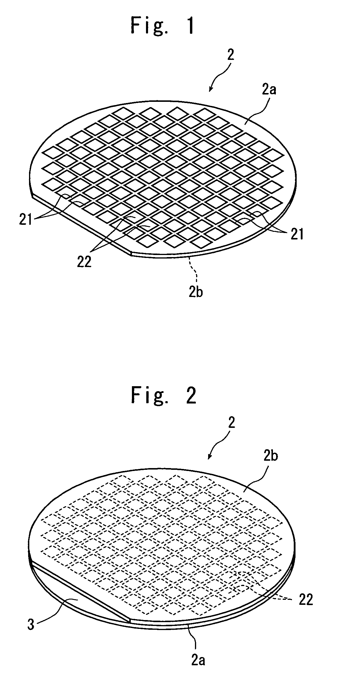
[0031]FIG. 1 is a perspective view of a semiconductor wafer as a wafer to be divided by the wafer dividing method of the present invention. The semiconductor wafer 2 shown in FIG. 1 is, for example, a silicon wafer having a thickness of 300 μm, and a plurality of dividing lines 21 are formed in a lattice pattern on the front surface 2a. A device 22 such as IC or LSI is formed in a plurality of areas sectioned by the plurality of dividing lines 21 on the front surface 2a of the semiconductor wafer 2. The method of dividing this semiconductor wafer 2 into individual semiconductor chips will be described hereinunder.

[0032]A protective member 3 is affixed to the front surface 2a of the above-described semiconductor wafer 2 as shown in FIG. 2 (protective member affixing step).

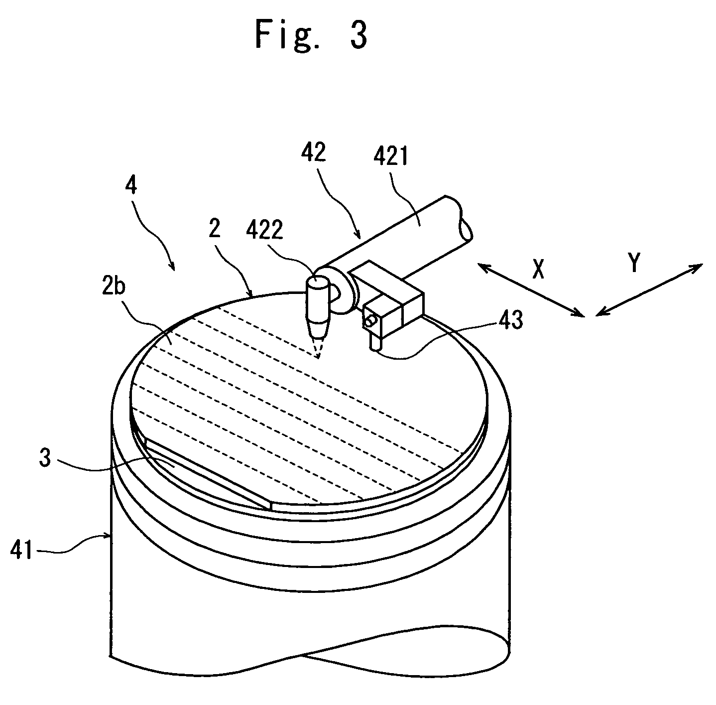
[0033]After the protective member 3 is affixed to...


PUM

PropertyMeasurementUnit
diameteraaaaaaaaaa
diameteraaaaaaaaaa
widthaaaaaaaaaa

Abstract

A method of dividing a wafer having devices formed in a plurality of areas sectioned by a plurality of dividing lines, into individual chips along the dividing lines, comprising a deteriorated layer forming step for forming a deteriorated layer by applying a laser beam of a wavelength having permeability for the wafer along the dividing lines; a wafer supporting step for putting the rear surface of the wafer on the surface of an adhesive tape which is mounted on an annular frame and whose adhesive strength is reduced by applying ultraviolet radiation thereto; and a chips-spacing forming step for reducing the adhesive strength of the adhesive tape and shrinking a shrink area between the inner periphery of the annular frame and the area to which the wafer has been affixed, of the adhesive tape by applying ultraviolet radiation to the adhesive tape to which the wafer has been affixed so as to divide the wafer into individual chips along the dividing lines where the deteriorated layer has been formed and widen the space between adjacent chips.

Description

FIELD OF THE INVENTION[0001]The present invention relates to a method of dividing a wafer having a plurality of dividing lines which are formed in a lattice pattern on the front surface and devices which are formed in a plurality of areas sectioned by the plurality of dividing lines, into individual chips along the dividing lines.DESCRIPTION OF THE PRIOR ART[0002]In the production process of a semiconductor device, a plurality of areas are sectioned by dividing lines called “streets” which are arranged in a lattice pattern on the front surface of a substantially disk-like semiconductor wafer, and a device such as IC or LSI is formed in each of the sectioned areas. Individual semiconductor chips are manufactured by cutting this semiconductor wafer along the dividing lines to divide it into the areas having each a device formed therein. An optical device wafer comprising a gallium nitride-based compound semiconductor laminated on the front surface of a sapphire substrate is also cut a...

Claims


Application Information

Patent Timeline
Patent Type & Authority Patents(United States)
IPC IPC(8): H01L21/78
CPCB23K26/0057B23K26/4075B28D5/0011H01L21/78B23K26/40B23K26/53B23K2103/50
Inventor NAKAMURA, MASARU
Owner DISCO CORP
Why Eureka
Try Eureka