Mold, imprint method, and process for producing chip

a technology of imprinting method and mold, which is applied in the field of mold, imprinting method and process for producing chips, can solve the problem that the alignment structure is not readily visible, and achieve the effect of high-quality alignment with work

Inactive Publication Date: 2009-03-31
CANON KK
View PDF19 Cites 17 Cited by
  • Summary
  • Abstract
  • Description
  • Claims
  • Application Information

AI Technical Summary

Benefits of technology

[0054]According to the present invention, it is possible to provide a mold capable of a highly accurate alignment with the work.

Problems solved by technology

However, as a result of a study carried out by the inventors, the above-described alignment method has the following problem.
Accordingly, the difference in refractive index between the materials for the mold and the photocurable resin material is small, so that even when projections and recesses for an alignment structure are provided on the mold surface by processing the mold, the alignment structure is not readily visually recognized due to its contact with the photocurable resin material.

Method used


Image

  • Mold, imprint method, and process for producing chip
  • Mold, imprint method, and process for producing chip
  • Mold, imprint method, and process for producing chip

Examples


first embodiment

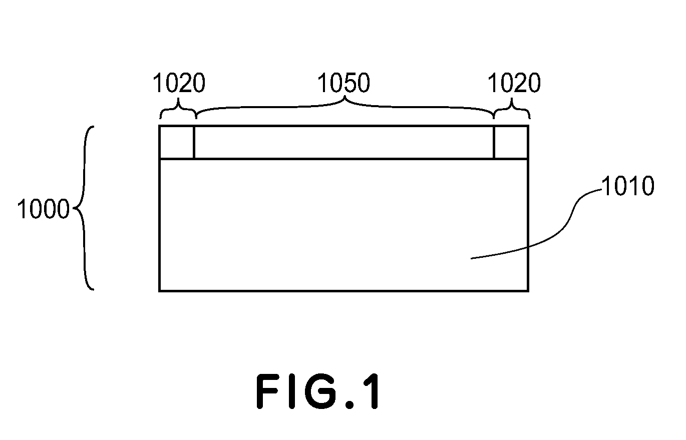
[0062]FIG. 1 is a schematic sectional view for illustrating an alignment mark provided in a mold (or a template).

[0063]Referring to FIG. 1, a mold 1000 includes a substrate (mold substrate) 1010, an alignment mark area 1020 in which an alignment mark is disposed, and a pattern area 1050 for transferring a pattern through imprint(ing). In the pattern area 1050, a pattern for imprint (e.g., a structure constituted by a recess and a projection) is actually formed, but is omitted from FIG. 1.

[0064]In this embodiment, the imprint pattern area 1050 is located at a central portion and two alignment mark areas 1020 are located at both sides of the imprint pattern area 1050, but a positional relationship therebetween is not particularly limited. For example, the alignment mark area 1020 may also be located inside the imprint pattern area 1050. Further, the number of the alignment mark areas 1020 may also be one or not less than three.

[0065]The alignment mark in this embodiment is utilized fo...

second embodiment

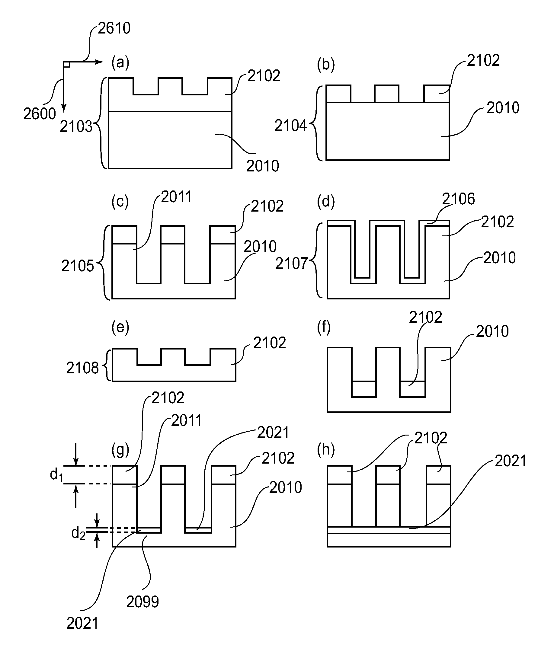
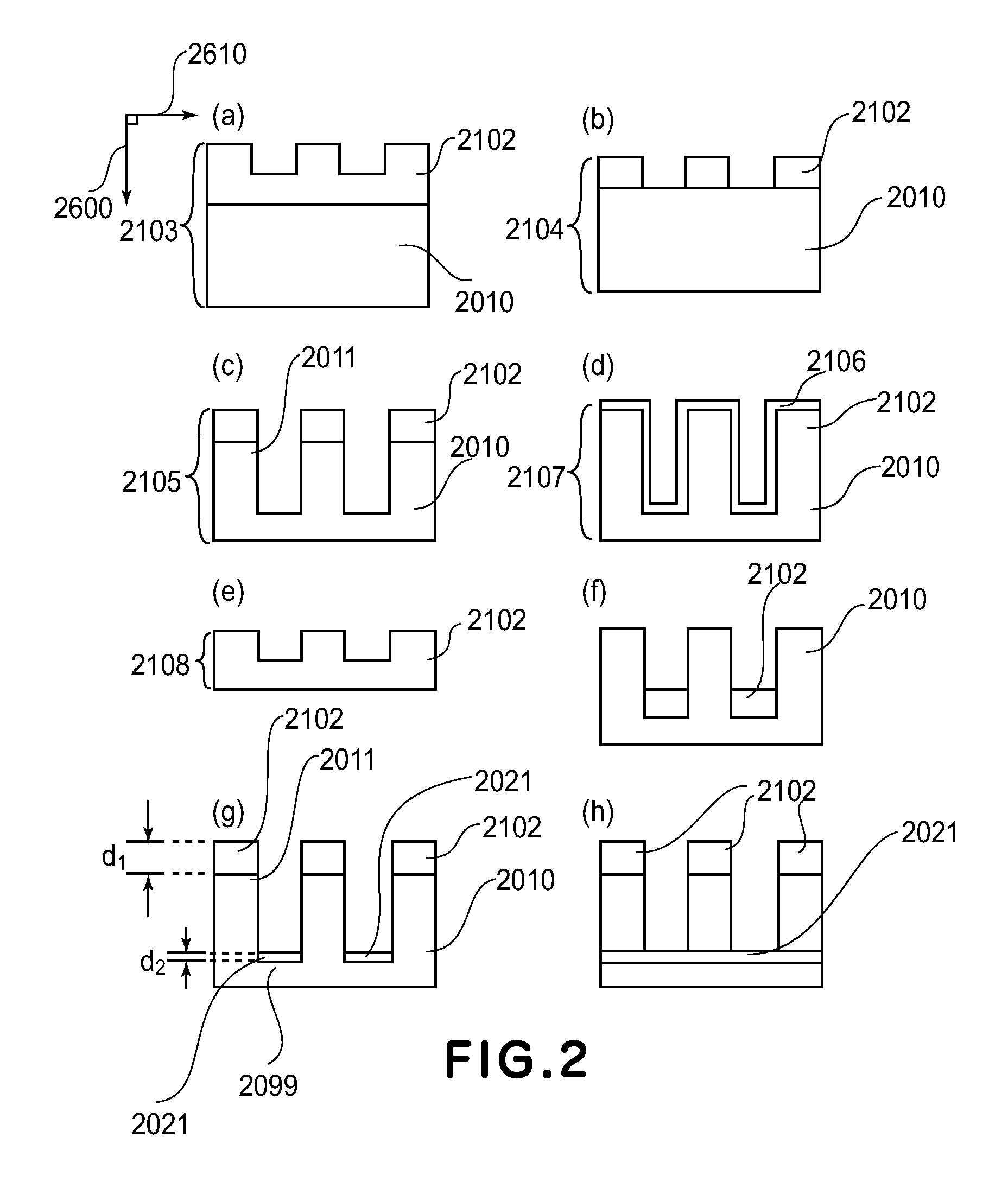
[0135]A mold according to Second Embodiment of the present invention will be described with reference to FIG. 2(g).

[0136]In the First Embodiment described above, FIG. 2(g) is the sectional view of the layer structure of the mold in the alignment mark area. However, in this embodiment, the layer structure shown in FIG. 2(g) is used without a distinction between the alignment mark area and the pattern area. This is because it is possible to appropriately determine, in some cases, whether or not a portion of an imprint pattern, having a recess and a projection, provided at a processing surface of the mold, is utilized as the alignment mark. More specifically, so long as the mold has features described below, the mold is embraced in the scope of the present invention irrespective of whether the features are provided in any area of the mold.

[0137]Referring to FIG. 2(g), the mold of this embodiment includes the substrate 2010 constituted by the first material, the plurality of recesses 20...

third embodiment

[0143]A mold according to this embodiment will be described with reference to FIG. 1. As shown in FIG. 1, the mold includes the imprint pattern area 1050 (in which a pattern of a recess and a projection is not shown) and the alignment mark area (in which an alignment mark is not shown). As described in the First Embodiment, the positional relationship between the respective areas and the number of the alignment mark area is not particularly limited.

[0144]The material constituting the alignment mark area is a material having a refractive index of not less than 1.7 and can be selected from, e.g., silicon nitride, titanium oxide, and aluminum oxide, described above. It is not necessary to form the alignment mark area only from the above-described material.

[0145]The imprint pattern area 1050 may be formed from the same material as described above or quartz (silica or fused silica).

[0146]By employing a constitution such as described above, e.g., even in the case where the processing surf...


PUM

PropertyMeasurementUnit
refractive indexaaaaaaaaaa

Abstract

A mold capable of effecting alignment of the mold and the member to be processed with high accuracy even in such a state that a photocurable resin material is disposed between the mold and the member to be processed is constituted by a substrate 2010 formed of a first material and an alignment mark 2102 formed of a second material different from the first material. The first material and the second material have transmittivities to light in a part of an ultraviolet wavelength range of the ultraviolet light. The second material has a refractive index of not less than 1.7.

Description

FIELD OF THE INVENTION AND RELATED ART[0001]The present invention relates to a mold, an imprint method using the mold, and a process for producing a chip by using the mold.[0002]In recent years, fine-processing technology for transferring a fine structure on a mold onto a member to be processed, such as a resin material or a metal material, under pressure has been developed and has received attention. This technology is called nanoimprinting or nanoembossing and has a dissolution on the order of several nanometers. Therefore, there are growing expectations that it will become the next-generation semiconductor fabrication technology to be used in place of a light exposure apparatus, such as a stepper or a scanner.[0003]The technology can permit simultaneous processing of a three-dimensional structure on a wafer, so that it is expected to be applied to the following production technologies other than the semiconductor fabrication technology. For example, the technology is expected to ...

Claims


Application Information

Patent Timeline
Patent Type & Authority Patents(United States)
IPC IPC(8): B29C59/00
CPCB82Y10/00B82Y40/00G03F7/0002G03F7/0017G03F9/7042B29C59/00B29C59/022G03F7/2012
Inventor TERASAKI, ATSUNORISEKI, JUNICHISUEHIRA, NOBUHITOINA, HIDEKIOKUSHIMA, SHINGO
Owner CANON KK
Why Eureka
Try Eureka