Semiconductor device

a semiconductor device and semiconductor technology, applied in the field of semiconductor devices, can solve the problems of increasing the electric power consumption of the semiconductor device, increasing the electric power consumption, and the influence of crosstalk and skew caused by coupling capacitance between adjacent signal nets, and achieve the effect of advancing the hyperfine structure of the semiconductor device and suppressing the response delay

Inactive Publication Date: 2009-04-07
RENESAS ELECTRONICS CORP
View PDF19 Cites 106 Cited by
  • Summary
  • Abstract
  • Description
  • Claims
  • Application Information

AI Technical Summary

Benefits of technology

[0022]According to the present invention, it is possible to provide the semiconductor device of the smaller circuit area, while attaining the control of the threshold voltage of the substrate bias where the threshold voltage of the transistor is changed on the basis of the substrate bias.
[0023]Also, according to the conventional technique, in order to place metal interconnections in smaller region, it is required to make the wirings thinner or the interval between wirings narrower. As a result, the response delay tends to occur. According to the present invention, it is possible to provide the semiconductor device, which suppresses the response delay when the substrate bias is applied, while attaining the advancement of the hyperfine structure of the semiconductor device.

Problems solved by technology

There is a case that because of the hyperfine structure, a current density when a transistor is operated and a static leakage current are increased, which results in the increase in the electric power consumption of the semiconductor device.
Also, usually, in order to enhance the performance of the semiconductor device, the operational frequency is basically set higher, which consequently increases the electric power consumption.
On the other hand, in association with the advancement of the hyperfine structure and higher integration of the semiconductor device, the influences of crosstalk and skew caused by coupling capacitance between adjacent signal nets and the like has become unignorable.

Method used


Image

  • Semiconductor device
  • Semiconductor device
  • Semiconductor device

Examples


first embodiment

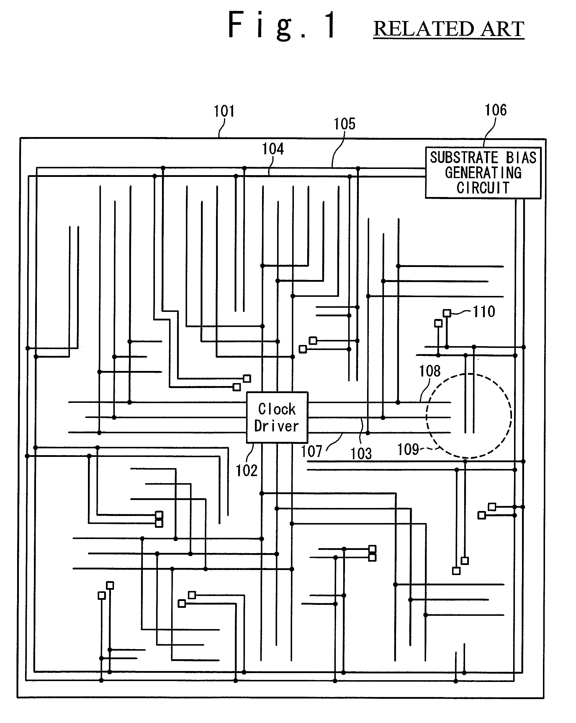
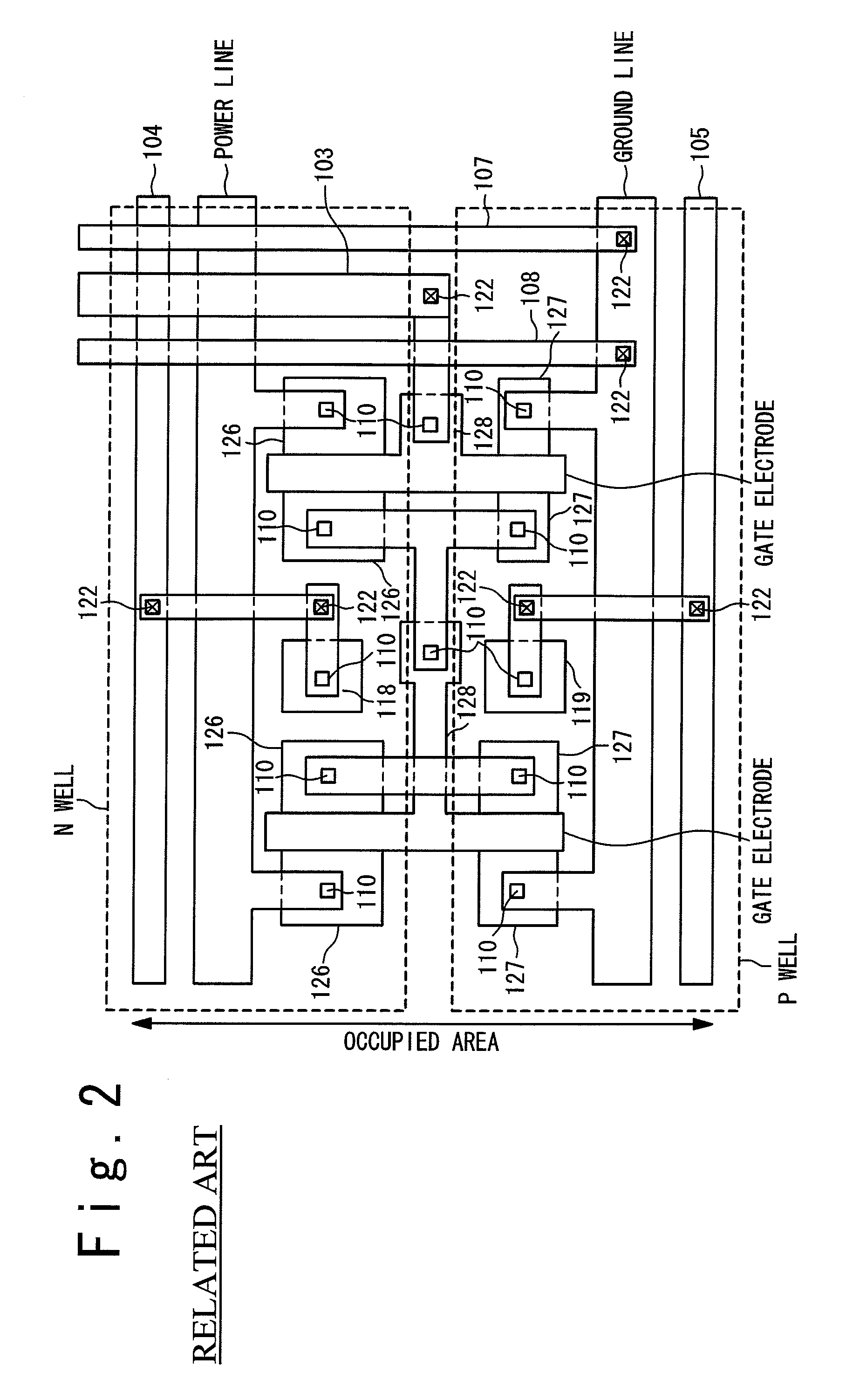
[0035]The embodiment of the semiconductor device of the present invention will be described below with reference to the drawings. In the following embodiments, it is supposed that the semiconductor device is the device which is constituted by one chip and has a normal mode in which normal operations are carried out and a standby mode in which operations except the minimum necessary operations are stopped for saving the electric power consumption.

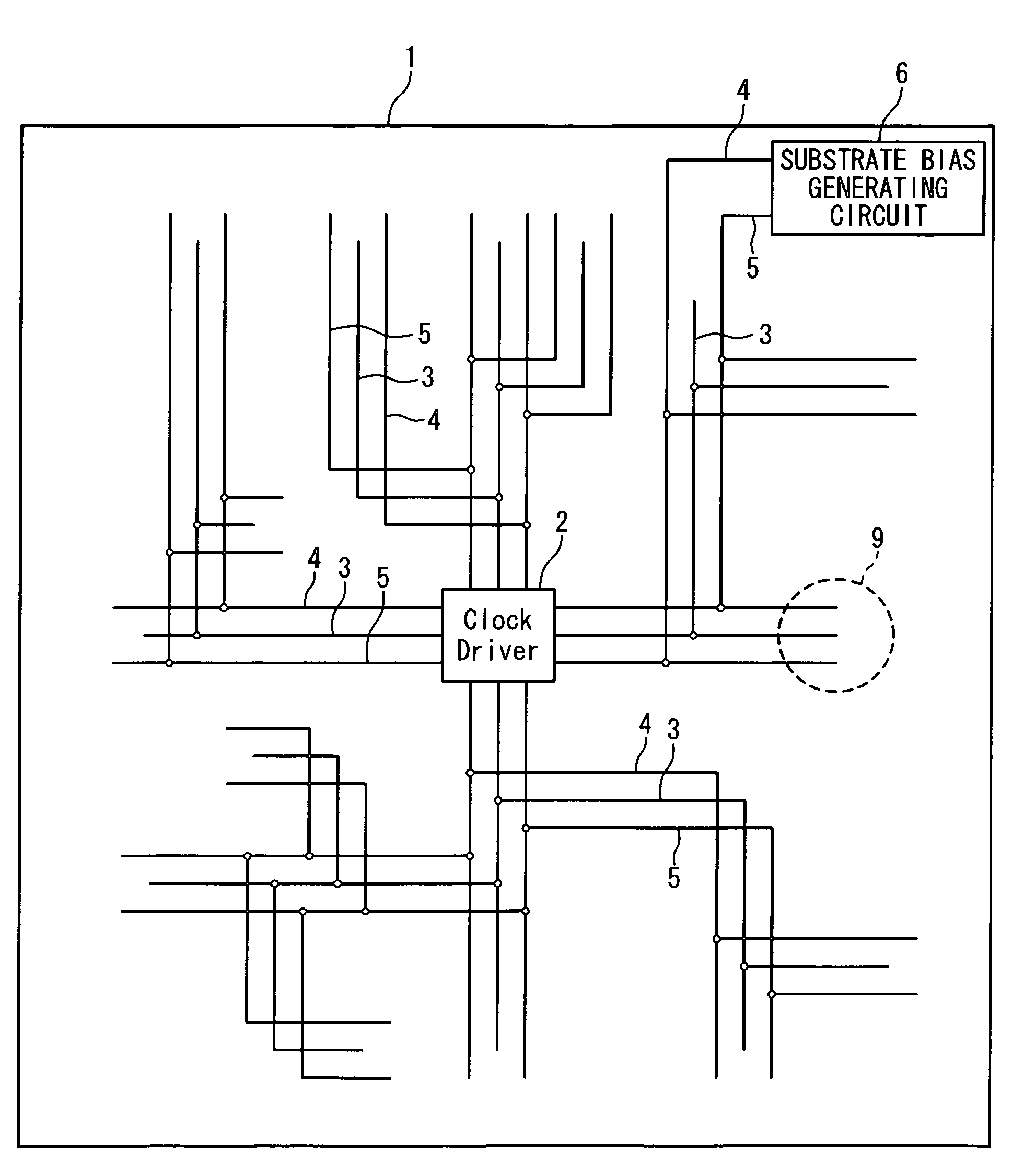
[0036]FIG. 3 shows a plan view of the semiconductor device 1 in this embodiment. With reference to FIG. 3, the semiconductor device 1 in the first embodiment contains a clock driver 2 and a clock line 3 for sending a clock signal outputted by the clock driver 2. Also, the semiconductor device 1 contains: an N-well side substrate bias supplying node 4 and a P-well side substrate bias supplying node 5 that are arranged along and in parallel with the clock line 3. As shown in FIG. 3, the N-well side substrate bias supplying node 4 and the P-wel...

second embodiment

[0054]The second embodiment of the present invention will be described below with reference to the drawings. In the following explanation, the members to which the same symbols as the symbols used in the explanation of the first embodiment are assigned have the similar configurations and operations. Thus, they are not explained in detail.

[0055]FIG. 7 is a plan view of the semiconductor device 1 according to the second embodiment of the present invention. With reference to FIG. 7, the substrate bias generating circuit 6 installed in the semiconductor device 1 of the second embodiment supplies the substrate bias to a particular region (for example, a substrate bias application region 10 shown in FIG. 7). There are semiconductor devices having a mixture of the region in which the threshold voltage is controlled through the substrate bias and the region in which such control is not required. In the second embodiment, when the semiconductor device 1 is the semiconductor device having suc...

third embodiment

[0057]The third embodiment of the present invention will be described below with reference to the drawings. In the explanation of this embodiment, the members to which the same symbols as the symbols used in the explanations of the other embodiments are assigned have the similar configurations and operations. Thus, they are not explained in detail.

[0058]FIG. 8 is a plan view of the semiconductor device 1 according to the third embodiment of the present invention. With reference to FIG. 8, the semiconductor device 1 in the third embodiment is provided with a plurality of substrate bias generating circuits 6. Although only two substrate bias generating circuits 6 are drawn in FIG. 8, the number of the substrate bias generating circuits can be set more than three. Under the condition that the signal delay is induced correspondingly to the advancement of the hyperfine structure of the semiconductor device, there is a case that the difference in the response speed is generated between th...


PUM


Abstract

A semiconductor device in which the threshold voltage of transistors is controlled through the applied substrate bias and having relatively small size. The semiconductor device includes: a clock signal line; a shield wiring for shielding the clock signal line from another interconnection; and a substrate bias generating circuit. The substrate bias is applied through the shield wiring to a region on which a transistor is formed. The threshold voltage of the transistor depends to the substrate bias applied to the transistor.

Description

BACKGROUND OF THE INVENTION[0001]1. Field of the Invention[0002]The present invention relates to a semiconductor device.[0003]2. Description of the Related Art[0004]In recent years, the advancement of the semiconductor manufacturing technique has promoted the miniaturization of semiconductor devices and the enhancement of the number of devices per unit area of a wafer. For example, in the case of manufacturing memory chips of the same storage capacity, the number of the chips that can be obtained from one silicon wafer can be increased, which can reduce the cost per chip. Also, in the case of manufacturing the memory chips of the same area, the storage capacity per chip can be increased, which enables a larger amount of information to be stored.[0005]There is a case that because of the hyperfine structure, a current density when a transistor is operated and a static leakage current are increased, which results in the increase in the electric power consumption of the semiconductor de...

Claims


Application Information

Patent Timeline
Patent Type & Authority Patents(United States)
IPC IPC(8): H01L39/00
CPCH01L23/5225H01L27/0207H01L27/11807H01L2924/0002H01L2924/00
Inventor YOSHIDA, MASATOSHI
Owner RENESAS ELECTRONICS CORP
Why Eureka
Try Eureka