Piezoelectric single crystal and piezoelectric single-crystal device and method for manufacturing the same

a single crystal, piezoelectric technology, applied in the direction of polycrystalline material growth, device material selection, generator/motor, etc., can solve the problems of high cost of piezoelectric single crystals. , to achieve the effect of improving the mechanical quality factor qm, suppressing the effect of deterioration over time and improving the relative dielectric constan

Inactive Publication Date: 2009-04-14
KAWATETABU MINING
View PDF6 Cites 4 Cited by
  • Summary
  • Abstract
  • Description
  • Claims
  • Application Information

AI Technical Summary

Benefits of technology

[0058]Advantageous effects of the addition of these elements are, for example, that the mechanical quality factor Qm can be improved and deterioration over time can be suppressed by adding Mn or Cr. In order to achieve these advantageous effects, one or more elements selected from Mn and Cr is preferably added in a content of 0.05 mol % or more in total. Additionally, the relative dielectric constant can be improved by adding Sb, La, W, or Ta. In order to achieve this advantageous effect, one or more elements selected from the group consisting of Sb, La, W, and Ta is preferably added in a content of 0.05 mol % or more in total. Furthermore, Al and Li contribute to stabilizing the growth of a single crystal. In order to achieve this advantageous effect, one of more elements selected from Al and Li is preferably added in a content of 0.05 mol % or more in total.
[0059]Impurities such as Fe, Pt, Au, Pd, and Rh from the raw material or a crucible may be mixed during the manufacturing process of the piezoelectric single crystal. Since these impurities inhibit the generation of the single crystal, it is desirable that the impurities content is controlled to 0.5 mol % or less in total.(7) Crystal Structure of Piezoelectric Single Crystal (Complex Perovskite Structure)
[0060]As a unit lattice of a solid solution single crystal schematically shown in FIG. 5, a crystal structure according to the present invention has a perovskite structure (RMO3) such that Pb ions are positioned at the vertices of the unit lattice; oxygen ions are positioned at the face centers of the unit lattice; and an M ion is positioned at the body center of the unit lattice. Additionally, it is necessary that the crystal structure is a complex perovskite structure of which the M ion positioned at the body center in FIG. 5 is composed of a plurality of element ions consisting of at least two elements (specifically, selected from Mg, Nb, Zn, Ti, and In) instead of one kind of element ion.
[0061]Furthermore, a structure disposing at least one of elements selected from the group consisting of Mn, Cr, Sb, W, Al, La, Li, and Ta at the body center position of the unit lattice or the position between lattices is also included in the scope of the present invention.
[0062]When a single-crystal plate cut out from a grown single-crystal ingot is in an unmodified state, the directions of electric dipoles in one domain are the same as each other in the polarization direction PD and in the directions orthogonal to the PD, but those of individual domains are in various different directions. Therefore, the single-crystal plate does not exhibit piezoelectricity and remains in an unpolarized state.
[0063]Consequently, the electric dipoles in a large number of domains are in various different directions until they are aligned in a polarization direction PD (in one direction) by selecting a polarizing temperature and an electric field to be applied, which are generally determined as polarization conditions, and polarizing by applying an electric field along the polarization direction PD. With this, for example, lead zinc niobate-lead titanate (PZN-PT) or lead magnesium niobate-lead titanate Pb(Mg1 / 3Nb2 / 3)O3—PbTiO3 (PMN-PT) can have a high electromechanical coupling factor k33 in the polarization direction PD of 80% or more.

Problems solved by technology

However, an ingot and a wafer (substrate) formed of a piezoelectric single crystal of lead zinc niobate-lead titanate (PZN-PT) is expensive compared with those formed of lead zirconium titanate (Pb(Zr, Ti)O3: PZT) which is a conventional piezoelectric device material.
Additionally, a piezoelectric single crystal formed of lead magnesium niobate-lead titanate (PMN-PT) using lead magnesium niobate (PMN) instead of lead zinc niobate (PZN) and other piezoelectric single crystals having a similar composition are also expensive.
A second cause is the occurrence of cracks during the single-crystal growth.
Cracking of the single crystal (heat cracking) tends to occur during the growth process and the cooling process due to thermal strain caused by these temperature differences.
Additionally, there is a tendency that the cracking occurs more readily in a single crystal having better crystallinity.
A third cause is the occurrence of chipping during the manufacturing of a piezoelectric single-crystal device.
Therefore, the single-crystal plate yield of the piezoelectric single-crystal device is significantly decreased.
Thus, when the piezoelectric single-crystal plate and the piezoelectric single-crystal device are manufactured by growing the piezoelectric single crystal using a powder, calcined material, or sintered compact of the raw material components for forming the piezoelectric single crystal, the decreases in the crystal yield and the wafer yield of the piezoelectric single-crystal device, and the single-crystal plate yield cannot be avoided and consequently the production cost is increased.
As a result, there have been negative effects such as the number of fields in which they can be applied is limited.

Method used


Image

  • Piezoelectric single crystal and piezoelectric single-crystal device and method for manufacturing the same
  • Piezoelectric single crystal and piezoelectric single-crystal device and method for manufacturing the same
  • Piezoelectric single crystal and piezoelectric single-crystal device and method for manufacturing the same

Examples


example 1

[0105]A [Pb(Ca)(Mg1 / 3Nb2 / 3)O3]0.65[Pb(Ca)(In1 / 2Nb1 / 2)O3]0.03[Pb(Ca)TiO3]0.32 (PMN65 / PIN03-PT32(Cal)) crystal of an example according to the present invention was grown by mixing powder of 65 mol % calcium-substituted lead magnesium niobate [Pb(Ca)(Mg1 / 3Nb2 / 3)O3] which was prepared by substituting Ca for 1 mol % lead (Pb) of 65 mol % lead magnesium niobate [Pb(Mg1 / 3Nb2 / 3)O3], 32 mol % lead titanate [PbTiO3], and 3 mol % lead indium niobate [Pb(In1 / 2Nb1 / 2)O3]; firing the resulting mixture; casting and putting it into a platinum crucible of 50 mm in diameter; heating it to 1350° C. in a vertical electric furnace to a melt; and solidifying it in one direction (Melt Bridgman method) by moving the crucible downward in a temperature gradient of 20° C. / cm at a rate of 0.5 mm / h.

[0106]For comparison, a lead magnesium niobate-lead titanate [Pb(Mg1 / 3Nb2 / 3)O3]0.68[PbTiO3]0.32 (PMN68-PT32) crystal of a comparative example was also grown by putting a sintered body of a solid solution composed of 6...

example 2

[0109]The two types of the wafers prepared in EXAMPLE 1 were processed into rectangular plates having an end face in a desired orientation. Here, the [001] direction is defined as the direction normal to a plane having the largest area of the wafer. Single-crystal plates of length 13 mm×width 4 mm×thickness 0.36 mm were cut out by using a dicing saw such that the directions normal to each end face reside in the [100] direction or the [010] direction. The single-crystal plates were prepared 50 pieces for each type of the wafers. The presence or absence of chipping when the two types of the wafers were processed, a ratio of the wafers with the chipping to the total (50 pieces), and a yield of the single-crystal plate (single-crystal plate yield=100%−chipping occurrence ratio) were investigated. Table 2 shows the results. The dicing process was performed at a cutting rate of 0.2 mm / s.

[0110]The presence or absence of the chipping was determined by observing the peripheries of the single...

example 3

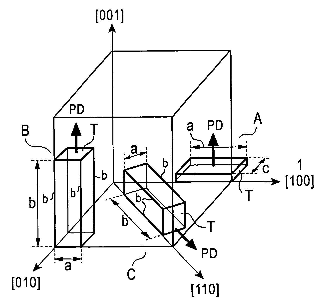
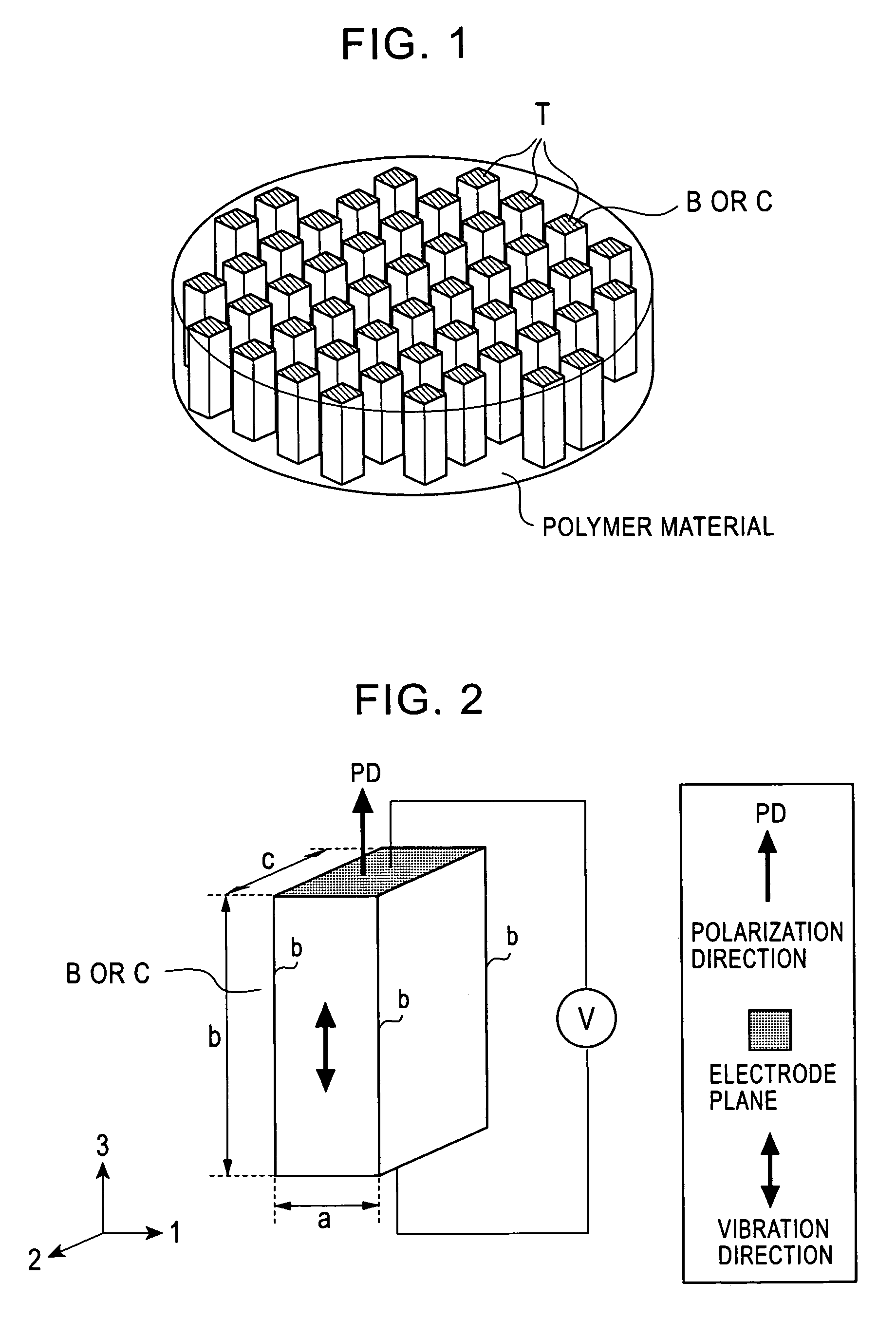
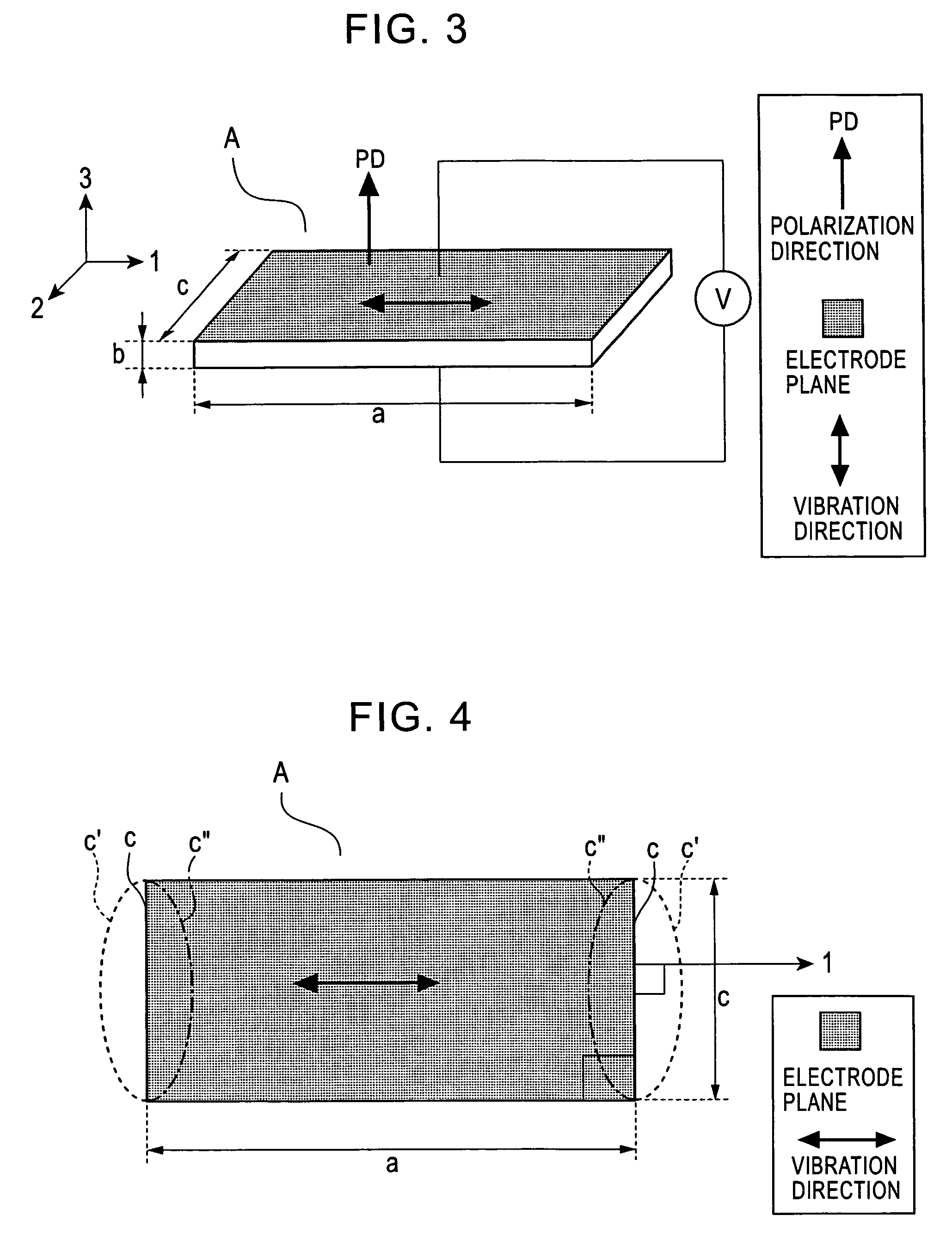
[0112]In order to produce piezoelectric single-crystal devices using a lateral vibration mode, single-crystal device materials of 13 mm×4 mm×0.36 mm were cut out from the two types of the wafers prepared in EXAMPLE 1 by using a dicing saw so as to have a size of 0.36 mm in the [001] direction, 4 mm in the [010] direction, and 13 mm in the [100] direction as shown in the single crystal device A in FIG. 6. Gold electrodes were produced on the opposing top and bottom faces in (100) planes of the produced single-crystal device material by forming a Cr—Au film (a first layer: Cr layer having a thickness of about 50 nm, a second layer: Au layer having a thickness of about 100 to 200 nm) by sputtering. Then, the single-crystal device material was put into a silicon oil bath of 40° C. and applied with a direct electric field of 700 V / mm for 1 hr for polarization. Thus, samples for evaluating piezoelectric characteristics were prepared. The piezoelectric characteristics, i.e., the electromec...


PUM

PropertyMeasurementUnit
temperatureaaaaaaaaaa
angleaaaaaaaaaa
angleaaaaaaaaaa

Abstract

An inexpensive piezoelectric single-crystal device being excellent in the piezoelectric characteristics and having a complex perovskite structure can be provided by adding a specific additive to a lead magnesium niobate-lead titanate (PMN-PT) single crystal or a lead zinc niobate-lead titanate (PZN-PT or PZNT) single crystal. Specifically, the piezoelectric single crystal has a complex perovskite structure and is formed of a composition containing 35 to 98 mol % lead magnesium niobate [Pb(Mg1 / 3Nb2 / 3)O3] or lead zinc niobate [Pb(Zn1 / 3Nb2 / 3)O3], 0.1 to 64.9 mol % lead titanate [PbTiO3], and 0.05 to 30 mol % lead indium niobate [Pb(In1 / 2Nb1 / 2)O3] wherein calcium is substituted for 0.05 to 10 mol % lead in the composition.

Description

TECHNICAL FIELD[0001]The present invention relates to piezoelectric single crystals and piezoelectric single-crystal devices and methods for manufacturing the same, and further relates to 1-3 piezoelectric composites as shown in FIG. 1.[0002]In particular, the present invention is a technology relating to an improvement in yield of piezoelectric single-crystal devices [for example, products formed of a lead magnesium niobate-lead titanate (Pb(Mg1 / 3Nb2 / 3)O3—PbTiO3: PMN-PT) single crystal or a lead zinc niobate-lead titanate (Pb(Zn1 / 3Nb2 / 3)O3—PbTiO3: PZN-PT or PZNT) single crystal] of which piezoelectric characteristics such as an electromechanical coupling factor (k31, k33) and a piezoelectric constant (d31, d33) are significantly improved compared with those of conventional sintered piezoelectric devices [for example, lead zirconium titanate (Pb(Zr, Ti)O3: PZT)].BACKGROUND ART[0003]When a piezoelectric single-crystal device is a rectangular parallelepiped, for example, as shown in F...

Claims


Application Information

Patent Timeline
Patent Type & Authority Patents(United States)
IPC IPC(8): H01L41/187C30B11/00C30B29/30C30B29/32H01L41/18H01L41/22H01L41/37H01L41/41
CPCC30B11/00C30B29/30C30B29/32H01L41/41H01L41/183H01L41/18H01L41/37Y10T29/42H10N30/85H10N30/852H10N30/095H10N30/092
Inventor MATSUSHITA, MITSUYOSHIIWASAKI, YOSUKE
Owner KAWATETABU MINING
Why Eureka
Try Eureka