Method for integrating DMOS into sub-micron CMOS process

a technology of cmos and dmos, which is applied in the direction of transistors, basic electric elements, electrical equipment, etc., can solve the problems of difficult to form pdmos, difficult to integrate dmos in sub, and high cost, and achieve the effect of easy addition

Active Publication Date: 2009-06-09
BCD SHANGHAI MICRO ELECTRONICS CO LTD
View PDF16 Cites 17 Cited by
  • Summary
  • Abstract
  • Description
  • Claims
  • Application Information

AI Technical Summary

Benefits of technology

[0011]This invention provides a solution by forming the DMOS channel after CMOS active layer while before gate poly layer to make the modular DMOS process step easily adding into the sub-micron CMOS or BiCMOS process. The advantages of this method are:

Problems solved by technology

Since the dopant diffusion needs high temperature drive while sub-micron CMOS (Complementary Metal Oxide Semiconductor) can not afford this thermal cycle, it is difficulty to integrated DMOS in sub-micron CMOS process forming a CDMOS process or sub-micron BiCMOS process forming a Bi-CDMOS process.
U.S. Pat. No. 5,491,105 is really a simple and cost effective method, but it is hard to form PDMOS due to diffusion rates of boron and arsenic are difference while phosphorous and boron are almost same.
U.S. Pat. No. 6,022,778 is also a very good method, but its cost is relatively high due to the polyside gate and large angle implant equipment.

Method used


Image

  • Method for integrating DMOS into sub-micron CMOS process
  • Method for integrating DMOS into sub-micron CMOS process
  • Method for integrating DMOS into sub-micron CMOS process

Examples


Embodiment Construction

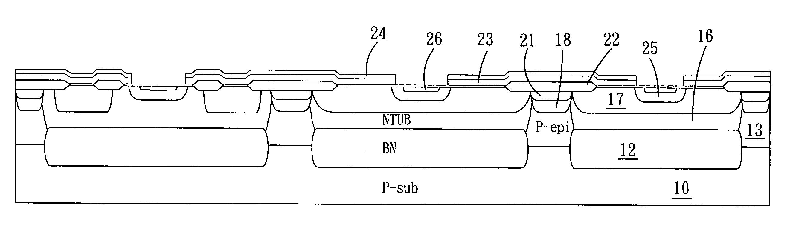
[0017]The technical contents of the present invention will be described below in detail via the exemplification of a NDMOS process and the attached drawings.

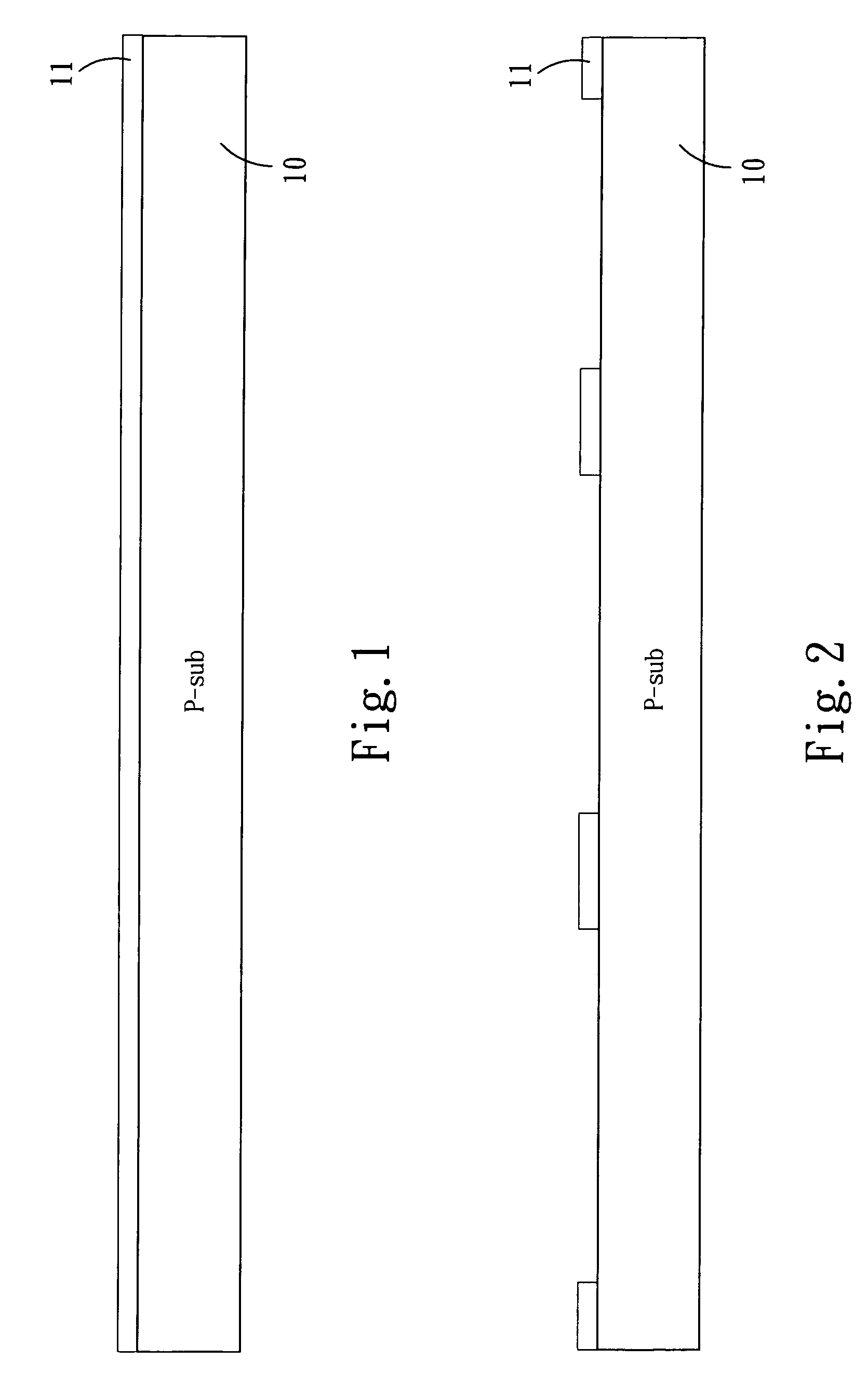
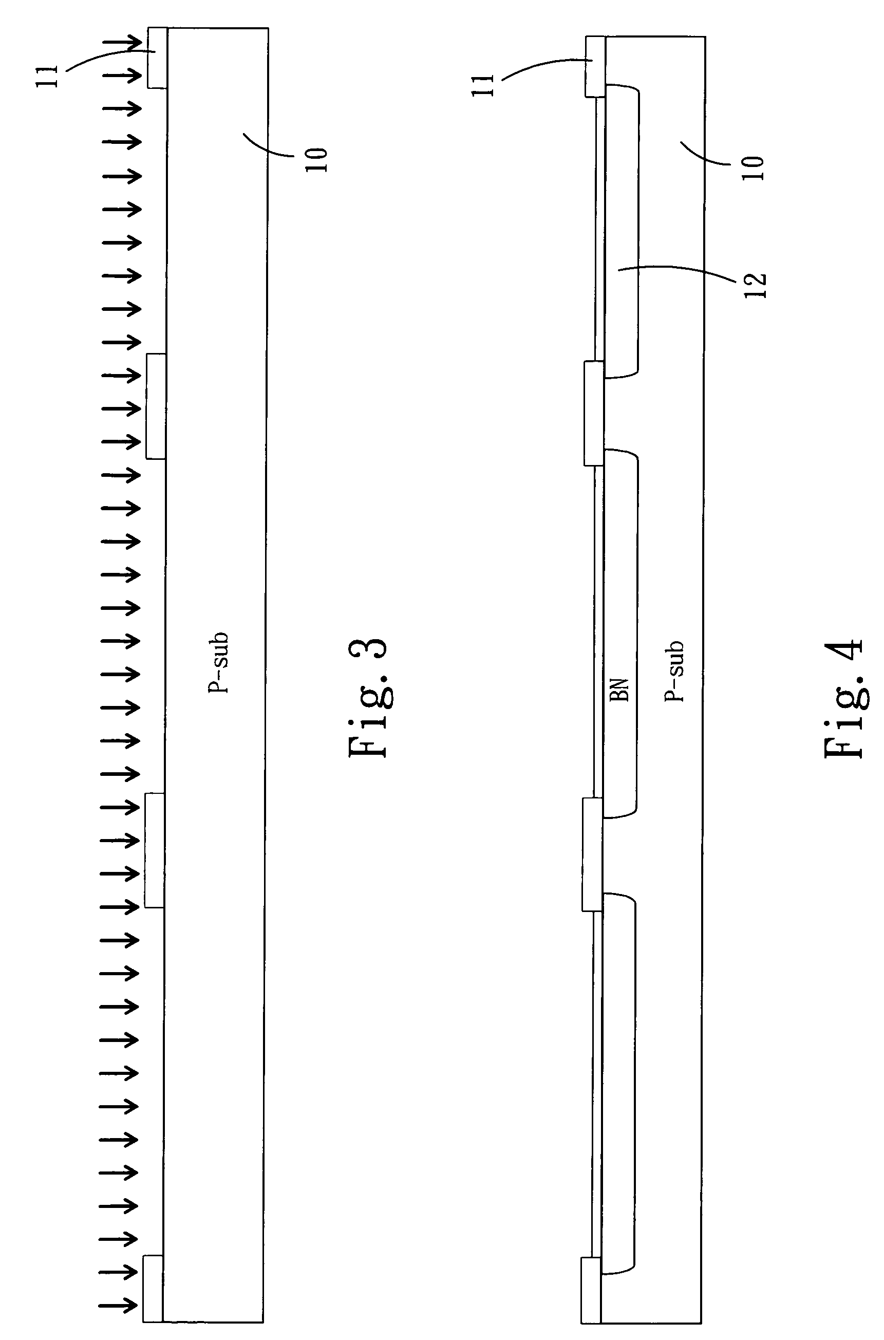
[0018]Refer to from FIG. 1 to FIG. 20 section views schematically showing the fabrication process of NDMOS. As shown in FIG. 1, a semiconductor substrate 10 (such as a P-substrate) is firstly provided, and an initial oxide layer 11 is formed on the surface of the substrate 10. Next, as shown in FIG. 2, via a lithographic process, the oxide layer 11 is selectively etched to form a shield mask of a required pattern, wherein some areas of the semiconductor substrate 10 are exposed, and N-type buried layers will be formed on the exposed areas of the substrate 10 in the following process.

[0019]Next, as shown in FIG. 3, N-type ions, such as Sb ions or As ions, are implanted into the exposed areas of the substrate 10, and then, as shown in FIG. 4, a drive-in process is performed to form N-type buried layers 12.

[0020]Next, as shown in F...


PUM


Abstract

This invention is forming the DMOS channel after CMOS active layer before gate poly layer to make the modular DMOS process step easily adding into the sub-micron CMOS or BiCMOS process. And DMOS source is formed by implant which is separated by a spacer self-aligned to the window for DMOS body. By this method, the performance of CMOS and bipolar devices formed original CMOS or BiCMOS process keeps no change. The product design kit, such as standard cell library of CMOS and BiCMOS, can be used continuously with no change.

Description

FIELD OF THE INVENTION[0001]The present invention relates to a fabrication method for semiconductor, particularly to a method for integrating DMOS into a sub-micron CMOS process or a sub-micron BiCOMS process.BACKGROUND OF THE INVENTION[0002]DMOS is the abbreviation of “Double Diffused Metal Oxide Semiconductor”, which can achieve a very high working frequency and a very high operational speed, wherein two dopants of opposite conductivity types are diffused through an identical window to form self-aligned sub-micron channels.[0003]According to DMOS structures, DMOS can be classified into LDMOS (lateral DMOS) and VMOS (vertical DMOS). LDMOS has three electrodes all extending from the upper surface thereof and is suitable to integrate with other elements. In a LDMOS, the source and the body are formed via a self-aligned diffusion; however, the gate layer and the drain are respectively formed via separated diffusion processes so that the input capacitor and the feedback capacitor can b...

Claims


Application Information

Patent Timeline
Patent Type & Authority Patents(United States)
IPC IPC(8): H01L21/20
CPCH01L21/823412H01L21/823418H01L21/823493H01L27/088H01L21/8249H01L27/0623
Inventor REN, CHONGLIU, XIAN-FENGTAO, HUANG HAI
Owner BCD SHANGHAI MICRO ELECTRONICS CO LTD
Why Eureka
Try Eureka