Manufacturing method for nitride semiconductor device and nitride semiconductor light emitting device obtained with the same

a manufacturing method and technology of nitride semiconductor, applied in semiconductor laser structure details, semiconductor lasers, manufacturing tools, etc., can solve problems such as difficult substrate cleavage, and achieve excellent lattice matching, high-performance semiconductor laser, and easy cracking.

Active Publication Date: 2009-07-28
ROHM CO LTD
View PDF6 Cites 76 Cited by
  • Summary
  • Abstract
  • Description
  • Claims
  • Application Information

AI Technical Summary

Benefits of technology

[0009]Another object of the present invention is to provide a manufacturing method for a nitride semiconductor device, where a wafer laminated nitride semiconductor layers can easily be divided into chips without fail by providing optimal conditions for dividing the wafer into chips in accordance with a multiple photons absorbing method.
[0031]Furthermore, since the wavelength and the intensity of the laser beam for irradiating as well as the depth where the substrate is irradiated can be optimized, a more precise cleavage can be provided. As a result, end faces of a resonator can be formed through the cleavage in an LD using a nitride semiconductor, and thereby, a very high performance semiconductor laser for emitting from blue to ultraviolet light can be obtained. Furthermore, in the case of an LED, a wafer can be very easily divided into chips for a device for emitting from blue to ultraviolet light having very hard nitride semiconductor layers grown on the substrate, and the wafer can be cut along the intended cutting lines without fail, and therefore, the number of wasted chips resulting from deviations in the cracking can be greatly reduced, increasing the yield, which greatly contributes to the reduction in cost. Here, dividing into chips for transistors also becomes very easy, leading to a reduction in the cost.

Problems solved by technology

As a result, it is difficult to cleave the substrate.

Method used


Image

  • Manufacturing method for nitride semiconductor device and nitride semiconductor light emitting device obtained with the same
  • Manufacturing method for nitride semiconductor device and nitride semiconductor light emitting device obtained with the same
  • Manufacturing method for nitride semiconductor device and nitride semiconductor light emitting device obtained with the same

Examples


Embodiment Construction

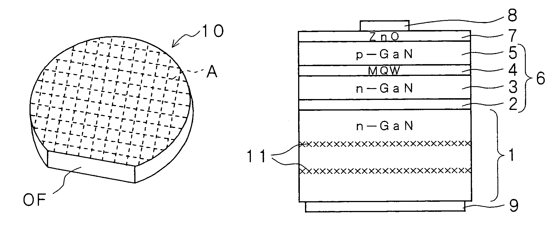
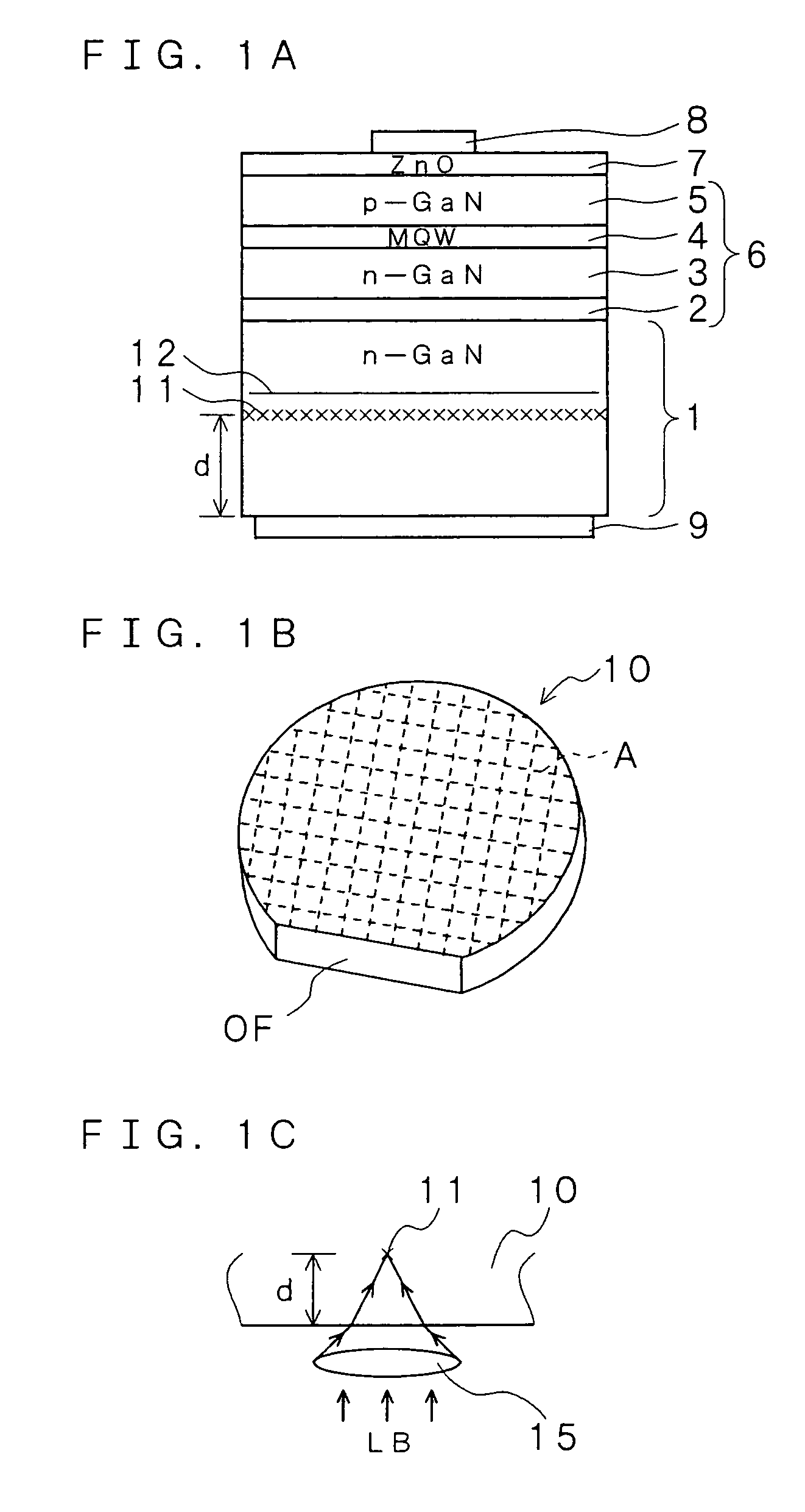
[0042]Next, a manufacturing method for a nitride semiconductor device according to the present invention and a nitride semiconductor light emitting device which is obtained in accordance with this manufacturing method are described in reference to the drawings. As for the nitride semiconductor device according to the present invention, FIG. 1A is a cross sectional diagram showing a nitride semiconductor light emitting device (LED chip) that has been divided into chips according to one embodiment, and FIG. 1B is a perspective diagram showing a wafer on which intended cutting lines are drawn, and as shown in these respective figures, first, a semiconductor lamination portion 6 is formed of nitride semiconductor layers, which at least include an n-type layer 3 and a p-type layer 5, on a surface of a wafer 10 formed of a GaN based substrate 1, and next, as shown in FIG. 1C, which is a schematic diagram showing the radiation of a laser beam LB, at least a portion of intended cutting line...


PUM

PropertyMeasurementUnit
wavelengthaaaaaaaaaa
absorption coefficientaaaaaaaaaa
thicknessaaaaaaaaaa

Abstract

Processed traces are formed on at least a part of intended cutting lines A along which a wafer (10) where a nitride semiconductor lamination portion (6) is formed on a GaN based substrate (1) is divided into chips, by irradiating with a laser beam LB having a wavelength which is longer than the band gap wavelength of the GaN based substrate 1 and an electrical field intensity which causes a multiple photons absorption, while adjusting the focal point to a constant depth d within the GaN based substrate (1) from the back surface of the wafer. After that, the wafer (10) is divided into chips along cutting starting points (12) which are formed in the vicinity of the processed traces by hitting with an impact. As a result, the wafer can be easily divided into chips, and in particular, end faces of a resonator can be formed with cleavage planes when an LD is formed.

Description

FIELD OF THE INVENTION[0001]The present invention relates to a manufacturing method for a semiconductor device, such as a light emitting diode (LED), a laser diode (LD) or a transistor element using a nitride semiconductor, and a nitride semiconductor light emitting device obtained in accordance with this method. In particular, the invention relates to a manufacturing method for a nitride semiconductor device where a wafer is divided into chips with a plane of cleavage which is a mirror surface and the yield at the time of dividing is high, and a nitride semiconductor light emitting device obtained with this method.BACKGROUND OF THE INVENTION[0002]In recent years, nitride semiconductor light emitting devices such as blue light emitting diodes (LED's) and laser diodes (LD's) using a nitride semiconductor have been put into practice. An LED for emitting blue light using a nitride semiconductor in this manner is formed by, for example, as shown in FIG. 10, laminating a low temperature ...

Claims


Application Information

Patent Timeline
Patent Type & Authority Patents(United States)
IPC IPC(8): H01L21/78B23K26/38H01L21/338H01L29/778H01L29/812H01L33/06H01L33/32H01S3/00H01S5/02
CPCB82Y20/00H01S5/34333H01S5/0201H01L21/78H01L33/0075H01L33/0095H01S5/0202H01S5/22H01S5/2214
Inventor KOHDA, SHINICHI
Owner ROHM CO LTD
Why Eureka
Try Eureka