Pillar-to-pillar flip-chip assembly

a flip-chip and pillar technology, applied in the field of semiconductor devices, can solve the problems of high cost of gold bumps, reliability problems, and failure of electrical connection between chips and substrates, and achieve the effect of avoiding peeling or breaking of solder joints and reducing thermal stresses

Active Publication Date: 2009-08-04
POWERTECH TECHNOLOGY
View PDF5 Cites 148 Cited by
  • Summary
  • Abstract
  • Description
  • Claims
  • Application Information

AI Technical Summary

Benefits of technology

[0007]The main purpose of the present invention is to provide a pillar-to-pillar flip-chip assembly to reduce the thermal stresses exerted on the interfaces between the soldering material and the bump pads of a substrate caused by warpage due to CTE mismatching between a chip and a substrate to avoid peeling or breaks of solder joints.

Problems solved by technology

Once external stresses are encountered, the bumps will easily be broken leading to electrical connection failure between a chip and a substrate.
However, tin-lead solder bumps can not meet the regulations of RoHS of Europe for environmental issues and the cost of gold bumps is not only high but also getting higher and higher in the recent years.
Moreover, there are reliability issues if lead-free solder bumps directly replace the tin-lead solder bumps.
However, during high-temperature reflowing processes, tin-lead solder bumps are melted to form solder balls leading to electrical short caused by bridging between adjacent solder balls for fine-pitch with small-spacing applications, moreover, an appropriate flip-chip gap between a bumped chip and a substrate cannot be maintained by solder balls for normal underfilling processes.
However, during high-temperature thermal compression processes, gold bumps will easily be crashed and deformed and an appropriate flip-chip gap between a bumped chip and a substrate cannot be maintained for normal underfilling processes in fine-pitch applications, either.
Moreover, high-temperature processes will impact the functions of IC chips.
Therefore, for the existing flip-chip technology either tin-lead solder bumps or gold bumps, the flip-chip gap between a bumped chip and a substrate can not effectively be controlled where the flip-chip gap will easily change due to variation of processing parameters such as temperatures or pressures causing poor underfilling qualities such as voids leading to reliability issues.
As shown in FIG. 3, when the substrate 110 of the conventional flip-chip assembly mentioned above experiences warpage due to temperature differences, more thermal stresses will exert on the bump pads 114 than on the copper pillar 130 causing peeling or breaks at the solder-joint interfaces leading to electrical failure and the reliability of the flip-chip assembly is impacted.

Method used


Image

  • Pillar-to-pillar flip-chip assembly
  • Pillar-to-pillar flip-chip assembly
  • Pillar-to-pillar flip-chip assembly

Examples


Embodiment Construction

[0026]Please refer to the attached drawings, the present invention is described by means of embodiment(s) below.

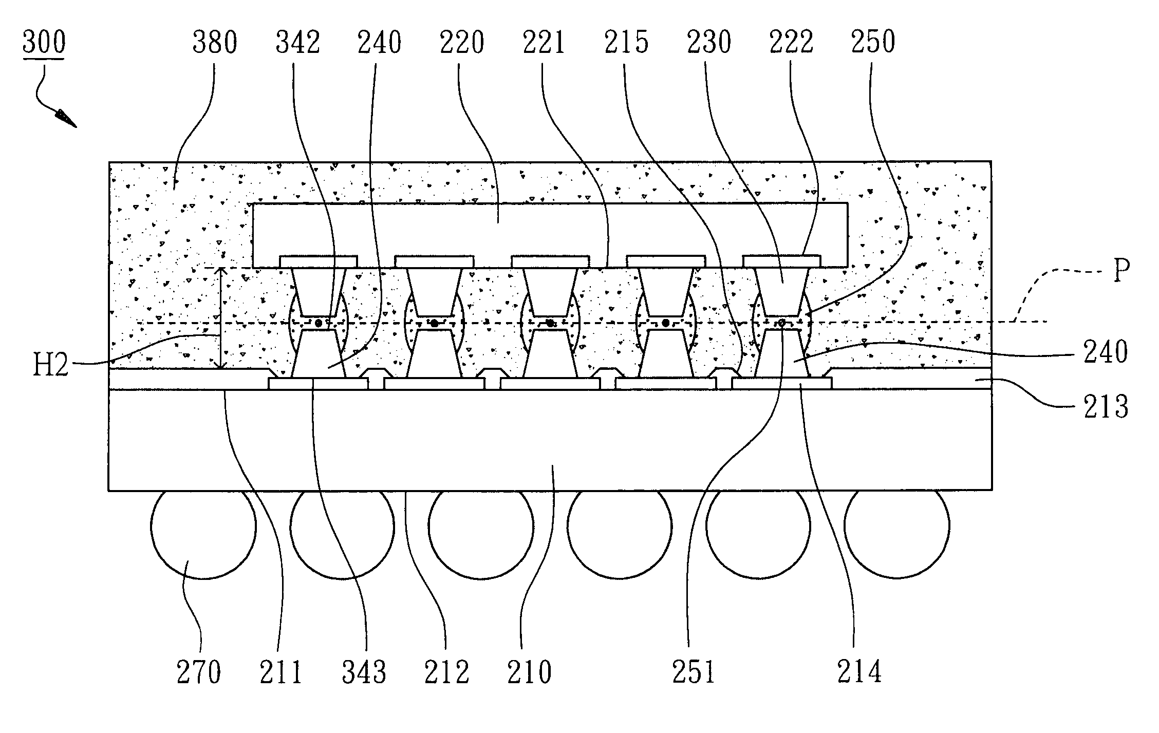
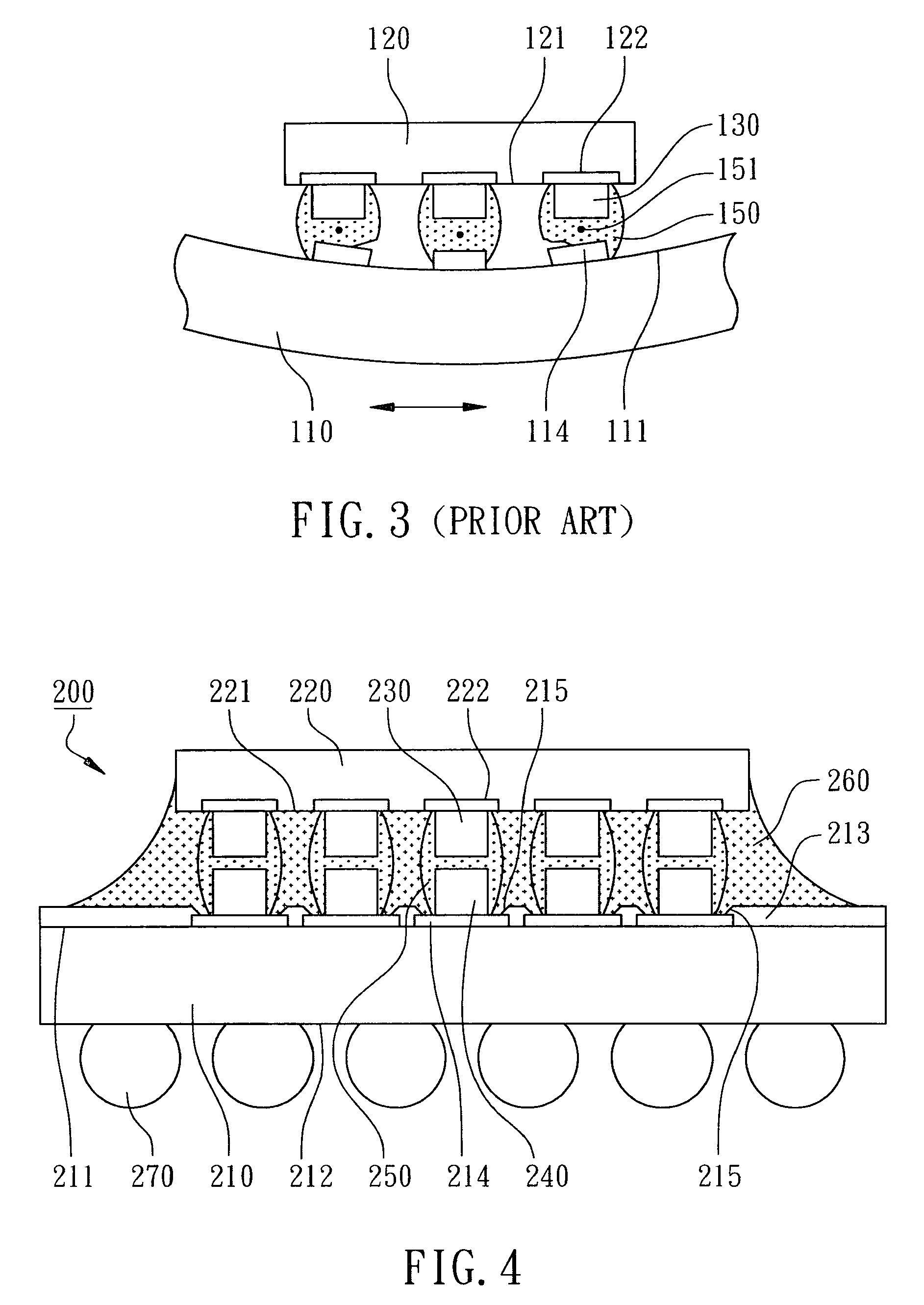
[0027]According to the preferred embodiment of the present invention, a pillar-to-pillar flip-chip assembly is illustrated in FIG. 4 for a cross-sectional view.

[0028]The pillar-to-pillar flip-chip assembly 200 primarily comprises a substrate 210, a chip 220, a plurality of first copper pillars 230, a plurality of second copper pillars 240, and a soldering material 250.

[0029]The substrate 210 has a top surface 211 and a corresponding bottom surface 212 which is a high-density, double-sided, multi-layer printed circuit board with internal conductive traces and vias manufactured. The substrate 210 can be one of the array units of a substrate strip and after package saw to become the substrate 210 described in the present embodiment. A solder mask 213 is formed on the top surface 211. A plurality of bump pads 214 are disposed on the top surface 211 with the bump pads 214 expos...


PUM


Abstract

A pillar-to-pillar flip-chip assembly primarily comprises a substrate, a chip disposed on the substrate, a plurality of first copper pillars on the bonding pads of the chip, a plurality of second copper pillars on the bump pads of the substrate, and a soldering material. A first height of the first copper pillars protruding from the active surface of the chip is the same as a second height of the second copper pillars from the solder mask on the substrate. When the soldering material electrically and mechanically connects the first copper pillars to the second copper pillars, a plurality of central points of the soldering material are formed on an equal-dividing plane between the chip and the substrate to reduce the direct stresses exerted at the soldering material to avoid peeling or breaks from the bump pads. Moreover, each of conventional solder balls is replaced with two soldered copper pillars to meet the lead-free requirements with higher reliability and lower costs.

Description

FIELD OF THE INVENTION[0001]The present invention relates to a semiconductor device, and more particularly to a pillar-to-pillar flip-chip assembly.BACKGROUND OF THE INVENTION[0002]Flip-chip technology is to dispose a plurality of conductive bumps or extruded electrical terminals on the bonding pads formed on the active surface of a chip, and then to flip the bumped chip onto a substrate to complete electrical connections. Comparing to the electrical connections by wire bonding, the flip chip technology provides shorter electrical connections between a chip and a substrate to enhance and achieve a higher signal transmission rate with a better signal quality for high-speed IC chips. Therefore, flip-chip technology becomes the trend for advanced semiconductor packages to provide higher operation speeds and better electrical performance. However, the flip-chip bonding between a chip and a substrate is point-to-point electrical connection. Once external stresses are encountered, the bum...

Claims


Application Information

Patent Timeline
Patent Type & Authority Patents(United States)
IPC IPC(8): H01L29/40
CPCH01L24/16H01L24/81H05K3/3436H01L24/13H01L21/563H01L2924/00013H01L2224/13012H01L2224/13016H01L2224/1308H01L2224/13082H01L2224/13111H01L2224/13147H01L2224/16H01L2224/81193H01L2224/812H01L2224/81801H01L2924/01015H01L2924/01029H01L2924/01078H01L2924/01079H01L2924/01082H01L2924/14H01L2924/1433H01L2924/15311H01L2924/3511H05K2201/0367H05K2201/0379H05K2201/10674H05K2201/10977H01L21/565H01L2224/73204H01L2224/32225H01L2224/16225H01L2924/0105H01L2924/01047H01L2924/01033H01L2924/01006H01L2924/00014H01L2224/13099H01L2924/00H01L2224/29099H01L2924/00012H01L24/05H01L24/06H01L2224/05001H01L2224/05022H01L2224/05572H01L2224/056H01L2224/16058H01L2224/1703H01L2224/17051H01L2924/181Y02P70/50H01L2224/05099
Inventor FAN, WEN-JENG
Owner POWERTECH TECHNOLOGY
Why Eureka
Try Eureka