Butted source contact and well strap

a source contact and well strap technology, applied in the direction of semiconductor devices, semiconductor/solid-state device details, electrical apparatus, etc., can solve the problems of soft error rate, interrupt the proper functioning of logic or memory devices, and the loss of logic devices and memory devices

Active Publication Date: 2009-09-08
TAIWAN SEMICON MFG CO LTD
View PDF4 Cites 26 Cited by
  • Summary
  • Abstract
  • Description
  • Claims
  • Application Information

AI Technical Summary

Benefits of technology

[0026]Thus, a structure and method for forming the same has been presented to form a butted contact forming both a source region contact and a well strap. Advantageously, according to the present invention the butted contacts decrease the required active area where separate well straps are formed as in prior art contact layout schemes, thereby allowing formation of well straps to each active region e.g., including each PMOSFET and / or NMOSFET active area in a semiconductor device or memory cell. The present invention additional enables improved device performance and reliability. For example, the soft error rate (SER) and latchup is reduced by supplying well straps in each MOSFET device or memory cell, e.g., one strap for each Vcc or Vss contact, thereby improved device stability and reliability. The contact layout structure including butted well straps of the present invention further provides a lower effective well resistance and decreased well strap length compared to prior art contact layout structures, thereby reducing subthreshold current leakage, improving device on current, and reducing bipolar transistor coupling effects.
[0008]To achieve the foregoing and other objects, and in accordance with the purposes of the present invention, as embodied and broadly described herein, the present invention provides A butted contact structure forming a source contact electrically connecting a voltage node and a well region and method for forming the same.

Problems solved by technology

Another increasingly important performance and reliability problem in logic and memory devices as device sizes decrease is the problem of latchup in logic devices and error rates in memory devices, also referred to as a soft error rate (SER).
The alpha or cosmic ray produced charge interferes with the proper functioning of a logic or memory device, for example static random access memory (SRAM) or dynamic random access memory (DRAM) devices.
For example it has been found that advanced SRAM devices are more susceptible to cosmic ray induced errors.
For example, a well region potential may become unstable if there is any leakage current in the well region.
An unstable well potential can correspondingly produce undesirable threshold or sub-threshold voltage instability.
One problem with fewer straps is an increase in the SER.
On the other hand, increasing the number of straps necessarily increases the size of the memory cell.

Method used


Image

  • Butted source contact and well strap
  • Butted source contact and well strap
  • Butted source contact and well strap

Examples


Embodiment Construction

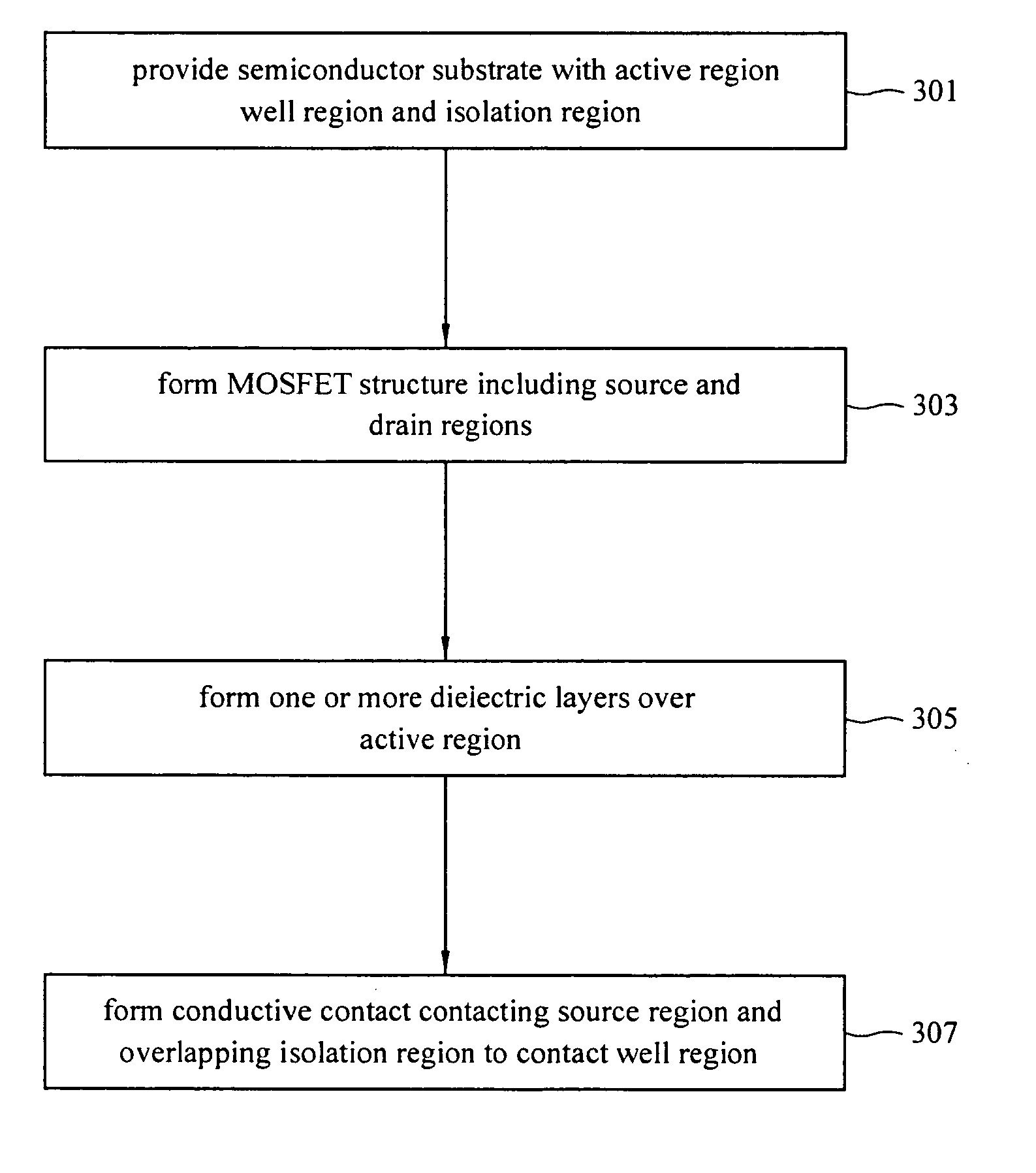
[0014]Although the method of the present invention is explained with reference to and is particularly advantageously implemented in forming low power MOSFET devices and static random access memory (SRAM) devices, it will be appreciated that the method of the present may be advantageously used to improve the performance of logic and memory devices in general, including reducing a soft error rate (SER), reducing latchup, improving device stability, reducing subthreshold current leakage, and reducing bipolar coupling effects. In addition, the present invention reduces a required active area to allow each active area well region to be electrically tied by a well strap to a respective voltage node.

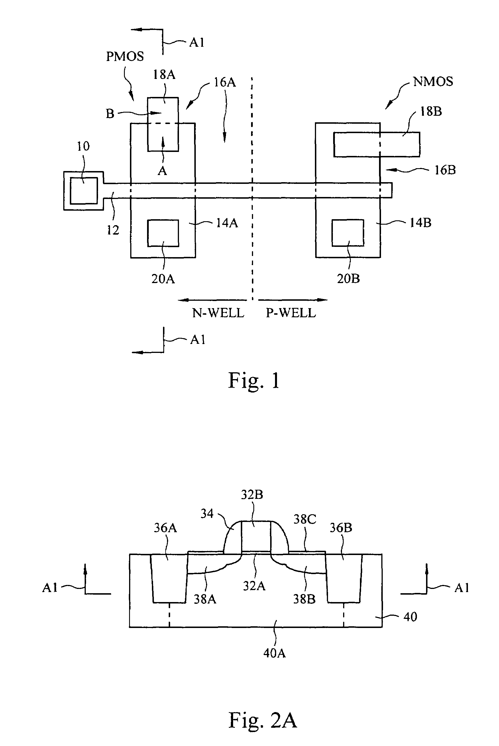
[0015]In an exemplary embodiment of the present invention, reference is made to FIG. 1 where a top planar view of a portion of a contact structure (contact layout) of PMOS and NMOS active regions (e.g., bipolar device) of a memory cell array is shown. For example, shown is gate contact region 1...


PUM


Abstract

A butted contact structure forming a source contact electrically connecting a voltage node and a well region and method for forming the same, the butted contact structure including an active region having a well region disposed adjacent an electrical isolation region on a semiconductor substrate; a MOSFET device including a source and drain region on the active region; and, a conductive contact having a first portion formed to the source region and a second portion formed through the electrical isolation region to the doped well region.

Description

FIELD OF THE INVENTION[0001]This invention generally relates to semiconductor processing methods for forming contacts in a multilevel semiconductor device and more particularly a method for forming an improved well strap contact in a low power semiconductor logic and memory devices.BACKGROUND OF THE INVENTION[0002]As sizes of logic circuits and memory devices decreases together with a decrease in the operating Voltages, a decreasing amount of charge is stored in MOSFET devices and memory cells. For example in ultra low power devices, for example a static random access memory device (SRAM), requires periodic refresh signals to retain stored data where the ratio of standby current (Isb) to drive current (Idr) is a critical design parameter in low power devices to enable proper functioning.[0003]Another increasingly important performance and reliability problem in logic and memory devices as device sizes decrease is the problem of latchup in logic devices and error rates in memory devi...

Claims


Application Information

Patent Timeline
Patent Type & Authority Patents(United States)
IPC IPC(8): H01L21/00
CPCH01L21/743H01L21/76802H01L23/485H01L27/11H01L29/41766H01L21/28531H01L21/7624H01L21/76895H01L2924/0002H01L2924/00H10B10/00
Inventor LIAW, JHON-JHY
Owner TAIWAN SEMICON MFG CO LTD
Why Eureka
Try Eureka