Semiconductor device having a junction extended by a selective epitaxial growth (SEG) layer and method of fabricating the same

a technology of epitaxial growth and selective epitaxial expansion, which is applied in the direction of semiconductor devices, semiconductor/solid-state device details, electrical apparatus, etc., can solve the problems of short channel effect, slow operation speed, and need fine patterns, so as to increase the area of the junction, enhance the insulation characteristic of the isolation layer, and increase the leakage current

Active Publication Date: 2009-09-22
SAMSUNG ELECTRONICS CO LTD
View PDF9 Cites 12 Cited by
  • Summary
  • Abstract
  • Description
  • Claims
  • Application Information

AI Technical Summary

Benefits of technology

[0009]It is a feature of an embodiment of the present invention to provide a semiconductor memory device, in which the area of a junction can be increased without increasing leakage current.
[0010]It is another feature of an embodiment of the present invention to provide a semiconductor memory device, in which an insulation characteristic of an isolation layer is enhanced.

Problems solved by technology

This decrease causes a short channel effect, requires fine patterns, and slows operating speed.
Of these problems, the short channel effect is a particularly serious problem.
Also, thermoelectrons cause avalanche, and vertical electric fields deteriorate the mobility of carriers.
Further, the short channel effect increases an off current of a transistor, thereby degrading the refresh characteristic of a memory device.
However, as the area of a junction increases, the leakage current of the junction also increases.
An increase in leakage current deteriorates the refresh characteristic of a memory device.
Also, because a conventional FinFET has a small interval between fins, when an insulating isolation layer is filled in the interval, voids are formed in the filled insulating layer.
The voids have an adverse effect on the insulation characteristic of the isolation layer.
Moreover, the small interval between fins narrows an interval between active regions and further deteriorates the insulation characteristic of the isolation layer.

Method used


Image

  • Semiconductor device having a junction extended by a selective epitaxial growth (SEG) layer and method of fabricating the same
  • Semiconductor device having a junction extended by a selective epitaxial growth (SEG) layer and method of fabricating the same
  • Semiconductor device having a junction extended by a selective epitaxial growth (SEG) layer and method of fabricating the same

Examples


first embodiment

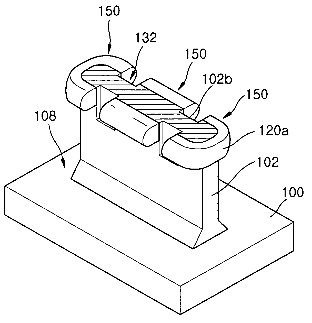
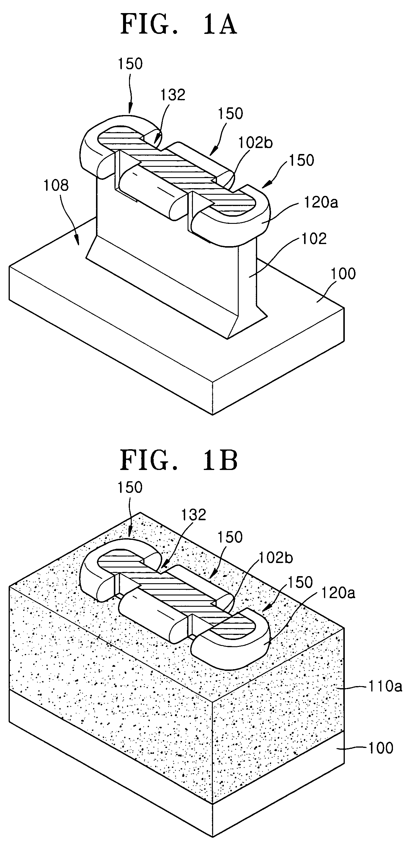
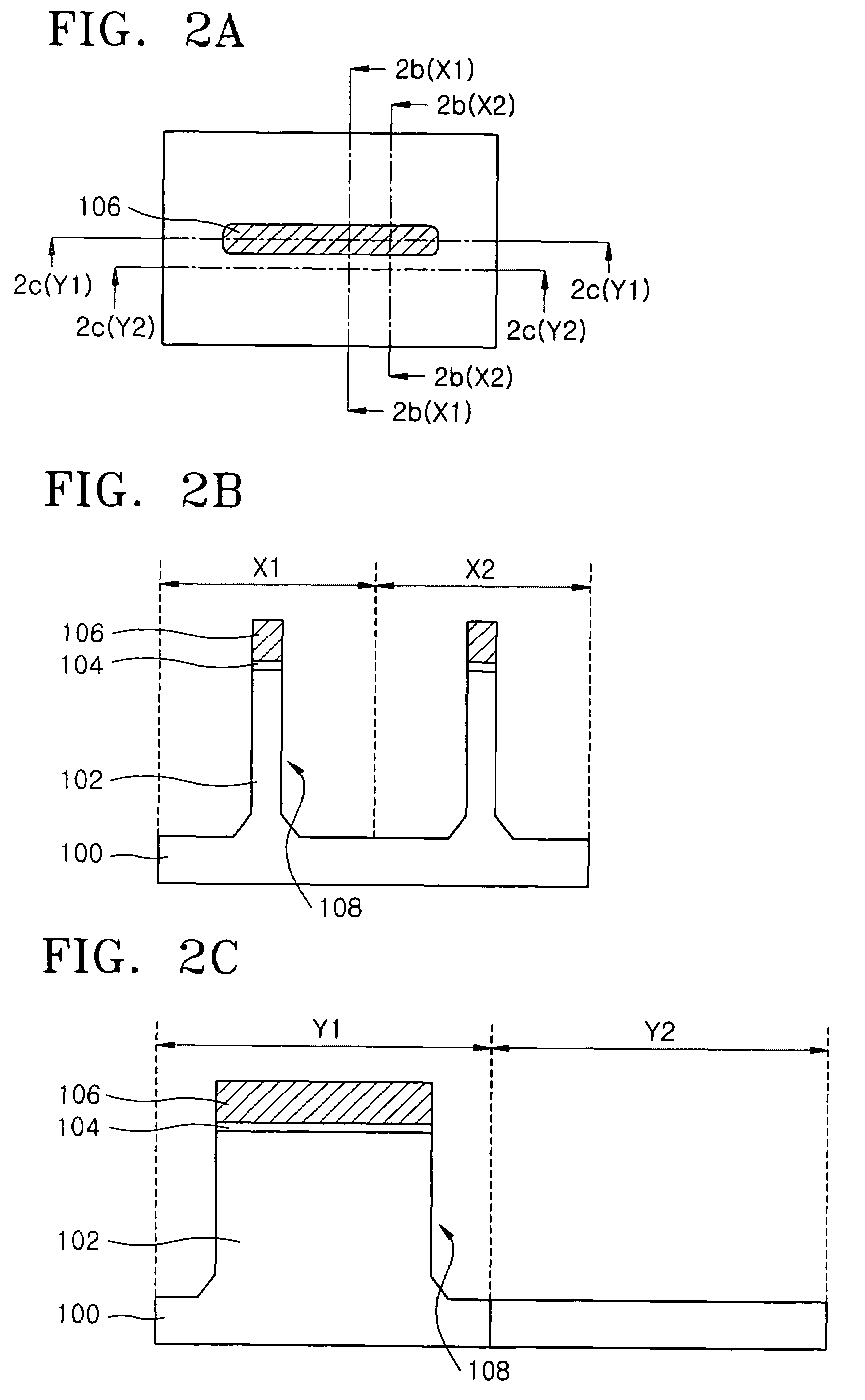
[0041]FIGS. 2A through 11A, 2B through 11B, and 2C through 11C illustrate stages in a method of fabricating a semiconductor device according to a first embodiment of the present invention.

[0042]FIG. 2A illustrates a plan view of a structure in which the protrusion 102 extends vertically from the semiconductor substrate 100. FIG. 2B illustrates cross-sectional views taken along x-axial lines 2b(X1) and 2b(X2) shown in FIG. 2A. FIG. 2C illustrates cross-sectional views taken along y-axial lines 2c(Y1) and 2c(Y2) shown in FIG. 2A.

[0043]Referring to FIGS. 2A through 2C, a pad oxide layer (not shown) and a nitride layer (not shown) for a mask are sequentially stacked on the semiconductor substrate 100. The pad oxide layer reduces stress between the substrate 100 and the nitride layer and is deposited to a thickness of about 20 to about 200 Å, preferably about 100 Å. The nitride layer is used as a hard mask during an etch process for forming a shallow trench isolation (STI) region and dep...

second embodiment

[0073]FIG. 12A illustrates a plan view of a structure after a width of an exposed protrusion 102a′ is reduced. FIG. 12B illustrates cross-sectional views taken along x-axial lines 12b(X1) and 12b(X2) shown in FIG. 12A. FIG. 12C illustrates cross-sectional views taken along y-axial lines 12c(Y1) and 12c(Y2) shown in FIG. 12A. In the second embodiment, a process of exposing the protrusion 102a′ is performed in the same manner as described in the first embodiment with reference to FIGS. 2A through 9A, 2B through 9B, and 2C through 9C.

[0074]The width of the exposed protrusion 102a′ may be reduced in order to control threshold voltage. Generally, a reduction in the width of the top surface of a channel region leads to a decrease in threshold voltage. If the width of the top surface of the channel region is greatly reduced and thus, the channel region is fully depleted, a threshold voltage is significantly reduced, e.g., to about one volt. Accordingly, if the threshold voltage does not re...


PUM


Abstract

In a semiconductor device, and a method of fabricating the same, the semiconductor device includes a protrusion extending from a substrate and a selective epitaxial growth (SEG) layer surrounding an upper portion of the protrusion, the SEG layer exposing sidewalls of a channel region of the protrusion.

Description

BACKGROUND OF THE INVENTION[0001]1. Field of the Invention[0002]The present invention relates to a semiconductor device and a method of fabricating the same. More particularly, the present invention relates to a semiconductor device having a junction extended by a selective epitaxial growth (SEG) layer and a method of fabricating the same.[0003]2. Description of the Related Art[0004]As semiconductor devices become more highly integrated, a channel length decreases. This decrease causes a short channel effect, requires fine patterns, and slows operating speed. Of these problems, the short channel effect is a particularly serious problem. For example, an increase in an electric field near a drain region leads to a punch-through, i.e., where a drain depletion region penetrates an electric potential barrier near a source region. Also, thermoelectrons cause avalanche, and vertical electric fields deteriorate the mobility of carriers. Further, the short channel effect increases an off cur...

Claims


Application Information

Patent Timeline
Patent Type & Authority Patents(United States)
IPC IPC(8): H01L29/06
CPCH01L21/02532H01L21/02603H01L21/0262H01L21/02631H01L29/66636H01L29/66818H01L29/7851H01L21/02639H01L29/7854H01L29/165H01L21/18
Inventor JANG, SE-MYEONGYANG, WOUN-SUCKYOON, JAE-MANSUNG, HYUN-JU
Owner SAMSUNG ELECTRONICS CO LTD
Why Eureka
Try Eureka