Beam homogenizer and laser irradiation apparatus and method of manufacturing semiconductor device

a laser irradiation and beam homogenizer technology, applied in the direction of manufacturing tools, instruments, gel state, etc., can solve the problems of inhomogeneity, striped pattern fade into the background, and the output of the laser oscillator is averaged, so as to increase the number of beams, and increase the uniformity of energy distribution

Inactive Publication Date: 2009-09-29
SEMICON ENERGY LAB CO LTD
View PDF63 Cites 18 Cited by
  • Summary
  • Abstract
  • Description
  • Claims
  • Application Information

AI Technical Summary

Benefits of technology

[0030]In the case where the light guide 1302 is present, incident light beams are reflected by the reflective surfaces of the light guide 1302 and all of them reach a region of the irradiation surface 1303b, as shown with the light beam 1301a. That is to say, in the case where the light guide 1302 is present, all of the incident light beams, which should reach regions of the irradiation surface 1303a and 1303c when the light guide 1302 is not present, reach a region of the irradiation surface 1303b. Accordingly, when a light beam is launched into the light guide 1302, the incident light beam is split and then all of the split beams are overlapped in the same location on the irradiation surface 1303b. Thus splitting an incident light beam to overlap the split light beams in the same l...

Problems solved by technology

The inhomogeneous energy distribution at the beam spot on the irradiated surface is caused by a structural problem and processing accuracy of the cylindrical lens array forming an optical system.
Namely, inhomogeneity arises from that all the laser beams induced into a homogenizer are not induced to the part where the cylindrical lenses function and tha...

Method used


Image

  • Beam homogenizer and laser irradiation apparatus and method of manufacturing semiconductor device
  • Beam homogenizer and laser irradiation apparatus and method of manufacturing semiconductor device
  • Beam homogenizer and laser irradiation apparatus and method of manufacturing semiconductor device

Examples


embodiment 1

[0064]An example of optical system other than the above-described optical system will be described here.

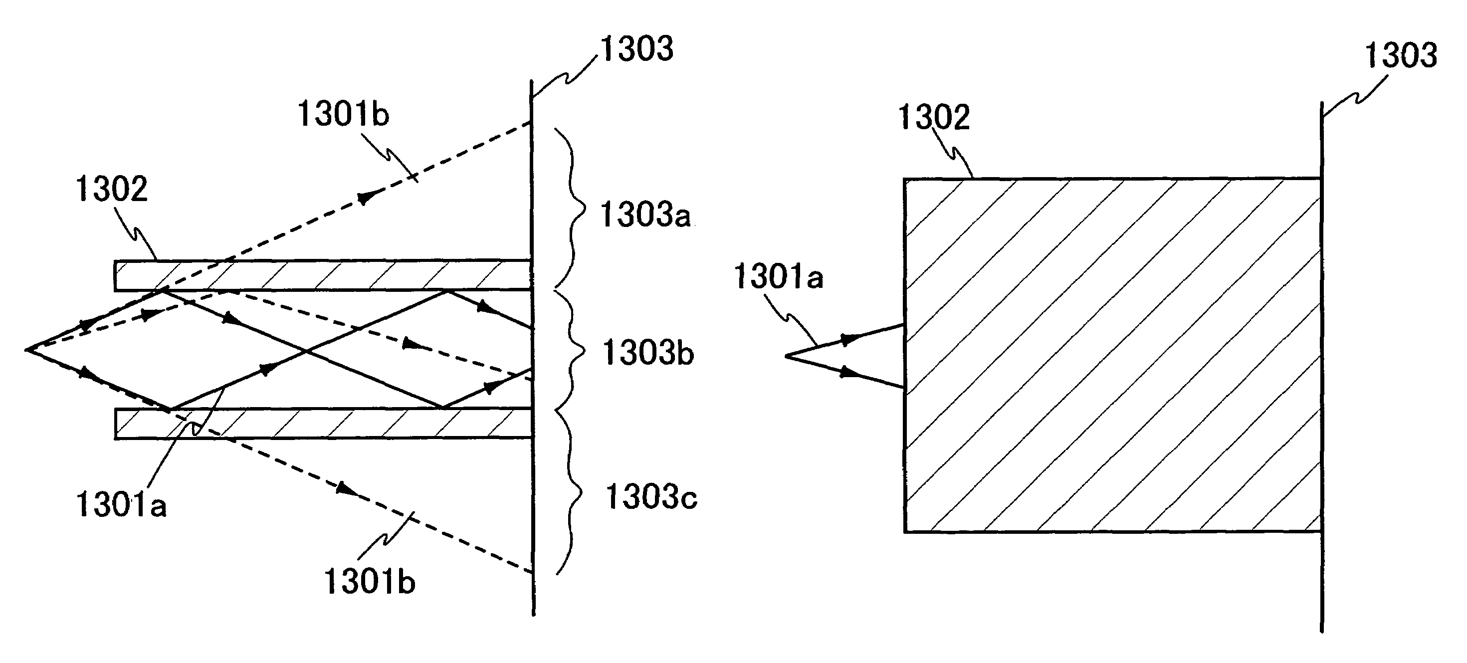
[0065]FIGS. 4A and 4B show an example of the optical system to be explained in this embodiment. First, a side view of FIG. 4B will be described. A laser beam emitted from the laser oscillator 1401 is propagated toward a direction of arrows indicated in the drawing. The beam spot is reduced in size in a direction of its shorter side using a 10 mm-thick cylindrical lens 1402 having a second surface of −182 mm in curvature radius. The light guide 1405, which has two reflective surfaces 1405a and 1405b facing to each other, is so placed that the beam inlet thereof lies in a focused area of the cylindrical lens. The light guide 1405 homogenizes the energy distribution of a beam spot. The light guide 1405 has a length of 300 mm in a direction in which a light beam travels and a distance of 0.4 mm between the reflective surfaces. An irradiation surface 1406 is placed at a location 0.2 mm...

embodiment 2

[0068]An example of optical system other than the above-described optical systems will be described here. FIGS. 6A and 6B show an example of the optical system to be explained in this embodiment.

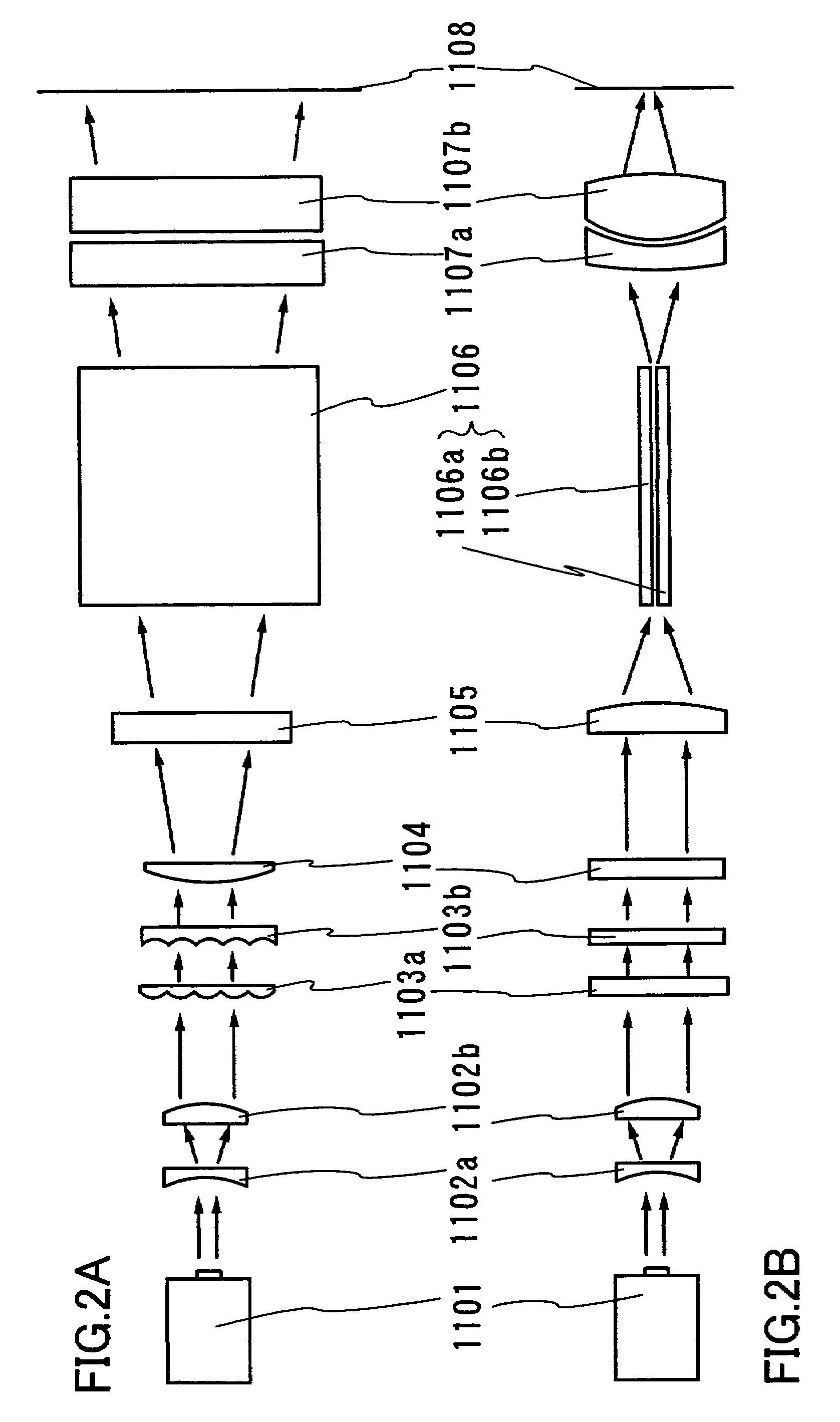
[0069]First, a side view of FIG. 6B will be described. In this drawing, a laser beam goes through exactly the same optical path as illustrated in FIGS. 4A and 4B until the laser beam reaches the light guide 1605 having two reflective surfaces 1605a and 1605b facing to each other. The light guide 1605 has two reflective surfaces facing to each other like the light guide 1405. The light guide 1605 measures 900 mm long in a direction in which a light beam travels and has a distance of 2.6 mm between the reflective surfaces. A light beam output from the light guide 1605 is shaped so as to form a rectangular beam spot measuring 2.6 mm in its shorter side with the energy distribution homogenized in a direction of the shorter side. The light beam output from the light guide 1605 is reduced in size ...

embodiment 3

[0073]An example of optical systems other than the above-described optical systems will be described here. FIGS. 8A and 8B show an example of the optical system to be explained in the embodiment.

[0074]In the drawings, a laser beam goes through exactly the same optical path as illustrated in FIGS. 4A and 4B except the light guide 1805. The light guide 1805 has two reflective surfaces facing to each other like the light guide 1405. The light guide 1405 has a hollow space between the two reflective surfaces facing to each other, whereas the light guide 1805 has a space filled with a medium 1805c having a refractive index of n between the reflective surfaces. This is different point between the two examples. In the case where the refractive index n of the medium is larger than that of the material from which the reflective surface is formed, a light beam is totally reflected off the reflective surface when the light beam enters the light guide 1805 at a angle smaller than or equal to th...


PUM

PropertyMeasurementUnit
Timeaaaaaaaaaa
Lengthaaaaaaaaaa
Distributionaaaaaaaaaa

Abstract

The inhomogeneous energy distribution at the beam spot on the irradiated surface is caused by a structural problem and processing accuracy of the cylindrical lens array forming an optical system.
According to the present invention, in the optical system for forming a rectangular beam spot, an optical system for homogenizing the energy distribution of the shorter side direction of a rectangular beam spot of a laser light on an irradiated surface is replaced with a light guide. The light guide is a circuit that can confine emitted beams in a certain region and guide and transmit its energy flow in parallel with the axis of a path thereof.

Description

BACKGROUND OF THE INVENTION[0001]1. Field of the Invention[0002]The present invention relates to a beam homogenizer which homogenizes a beam spot on a surface to-be-irradiated in a specified area, and further relates to a laser irradiation apparatus which irradiates a homogenized beam spot on a surface to-be-irradiated. Note that, a semiconductor device according to the present invention includes a display device such as an active matrix liquid crystal display device and an active matrix electro luminescence display device, an electro-optical device, and an electrical appliance utilizing such a display device or an electro-optical device, and the present invention also relates to a method of manufacturing the semiconductor device.[0003]2. Description of the Related Art[0004]Recently a technique of laser annealing that crystallizes or enhances crystallinity of an amorphous semiconductor film or a crystalline semiconductor film (a semiconductor film having crystallinity such as polycr...

Claims


Application Information

Patent Timeline
IPC IPC(8): C30B1/04H01L21/324B23K26/073G02B27/09
CPCB23K26/0639B23K26/0648B23K26/0732G02B27/09G02B27/0927G02B27/0994B23K26/0738Y10T117/1008B23K26/064H01L21/324
Inventor TANAKA, KOICHIRO
Owner SEMICON ENERGY LAB CO LTD
Why Eureka
Try Eureka