
Organic electroluminescent device

a technology of electroluminescent devices and organic materials, which is applied in the direction of discharge tube luminescnet screens, natural mineral layered products, etc., can solve the problems of high efficiency, inability to achieve white color, and inability to obtain light with a high luminance, etc., and achieve high efficiency

Active Publication Date: 2009-11-03
SANYO ELECTRIC CO LTD
View PDF17 Cites 20 Cited by
  • Summary
  • Abstract
  • Description
  • Claims
  • Application Information

AI Technical Summary

Benefits of technology

The present invention provides an organic electroluminescent device that can emit white light with high efficiency. The device comprises a light emitting layer containing two or more types of different luminescent materials, at least one of which is a phosphorescent material. The short wavelength light emitting layer mainly emits blue light, while the long wavelength light emitting layer mainly emits orange light. The two layers of the light emitting layer are connected to the first and second electrodes, respectively. The device can emit white light with high efficiency by supplying holes and electrons to the light emitting layer. The ratio of the first phosphorescent material to the first assisting dopant can be controlled to prevent high luminous intensity of the orange light. The energy levels of the highest occupied molecular orbit of the first host material, the first phosphorescent material, and the first assisting dopant can be optimized to achieve efficient white light emission.

Problems solved by technology

When white luminescence is realized using the blue luminescent material and the orange luminescent material, however, high efficiency as a white color cannot be realized unless the blue light and the orange light are emitted at a high efficiency.
On the other hand, when a white light emitting device and color filters are combined to perform full-color display, a part of white light is absorbed by the color filters, so that light having a high luminance is not obtained.

Method used


Image

  • Organic electroluminescent device
  • Organic electroluminescent device
  • Organic electroluminescent device

Examples


first embodiment

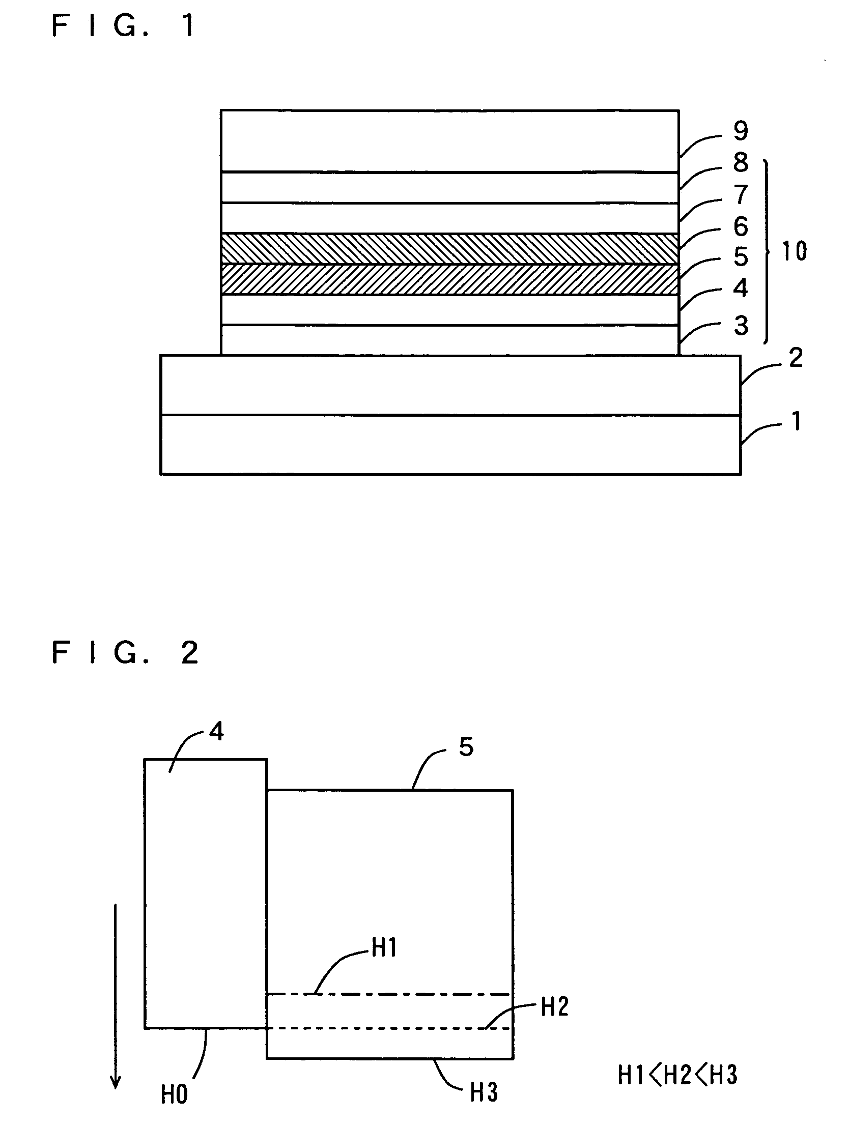
[0060]FIG. 1 is a schematic sectional view showing an organic EL device according to a first embodiment of the present invention.

[0061]In fabrication of an organic EL device 100 shown in FIG. 1, an anode 2 composed of In2O3—SnO2 (ITO) is previously formed on a glass substrate 1, and a hole injection layer 3, a hole transport layer 4, a blue light emitting layer 5, an orange light emitting layer 6, an electron transport layer 7, and an electron injection layer 8 are formed in this order by a vapor deposition at a vacuum in the 10−4 Pa order, to form an organic thin film layer 10. Further, a cathode 9 composed of an alloy of magnesium and indium (Mg:In) is formed on the organic thin film layer 10.

[0062]The hole transport layer 4 is composed of an amine-based material such as N,N′-Di(naphthalene-1-yl)-N,N′-diphenyl-benzidine (hereinafter referred to as NPB) having a molecular structure expressed by the following formula (D1), 4,4′4″-Tris(N-(2-naphthyl)-N-phenyl-amino)-triphenylamine (h...

second embodiment

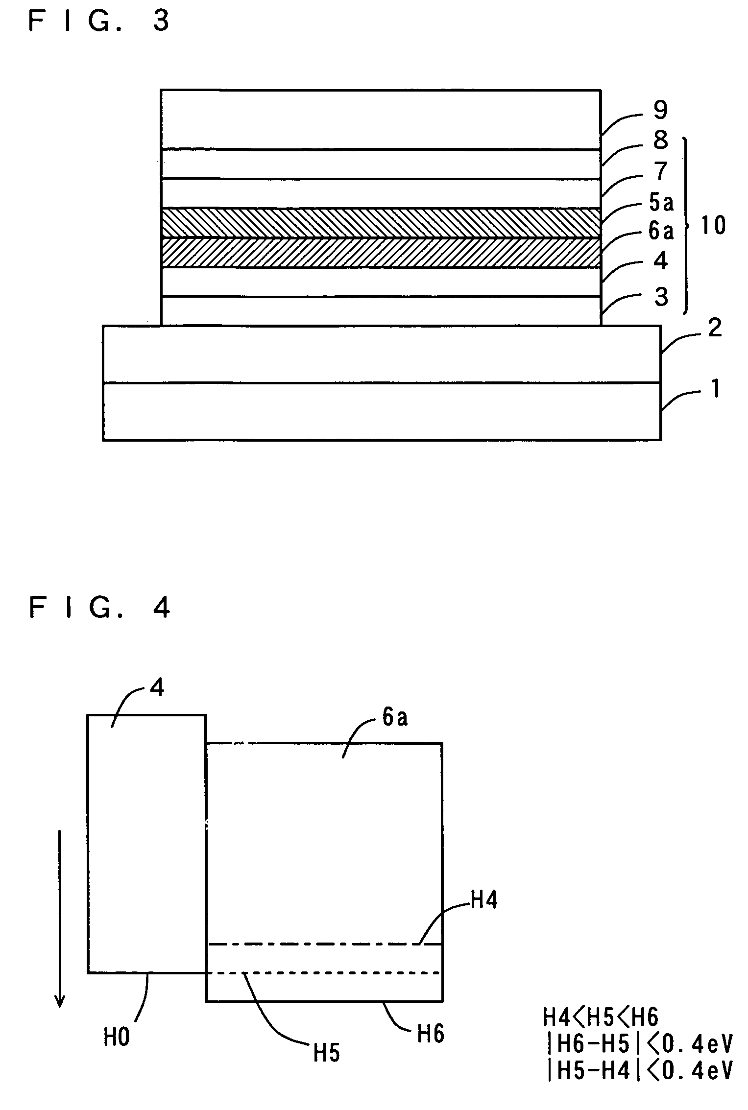
[0123]FIG. 3 is a schematic sectional view showing an organic EL device according to a second embodiment.

[0124]The organic EL device shown in FIG. 3 differs from the organic EL device shown in FIG. 1 in that a blue light emitting layer 5a and an orange light emitting layer 6a shown in FIG. 3 are formed in an order reverse to the blue light emitting layer 5 and the orange light emitting layer 6 shown in FIG. 1.

[0125]The orange light emitting layer 6a has a structure in which the assisting dopant is doped into the host material composing the orange light emitting layer 6 shown in FIG. 1. An example of an assisting dopant to be doped into a host material composing the orange light emitting layer 6a is NPB, Rubrene, or Ir(ppy) used for a hole transport layer 4.

[0126]In the orange light emitting layer 6a, the volume ratio of a luminescent dopant to the host material is approximately 6.5%, and the volume ratio of the assisting dopant thereto is 0% to 40%, for example. The volume ratio of ...

##ventive example 1

Inventive Example 1

[0138]In the inventive example 1, the organic EL device having the structure A was prepared. First, the anode 2 was formed on the glass substrate 1 by 80 nm sputtering. The glass substrate 1 having the anode 2 formed thereon was cleaned with a mild detergent and pure water, and was then baked at a temperature of 100° C. for not less than 10 hours, followed by UV / 03 cleaning, to set the glass substrate 1 in a chamber of a vacuum evaporation system which is depressurized to not more than 1×10⁻⁴ Pa.

[0139]CuPc was formed as the hole injection layer 3, and NPB was formed by vacuum evaporation as the hole transport layer 4. Then, the compound A was used as a host material, and TBP was used as a luminescent dopant, to form the blue light emitting layer 5. TBP was doped such that the volume ratio thereof to the blue light emitting layer 5 was 2%.

[0140]Then, CBP was used as the host material, and Ir(phq) was used as the luminescent dopant, to form the orange light emitting...


PUM

PropertyMeasurementUnit
peak wavelengthsaaaaaaaaaa
peak wavelengthaaaaaaaaaa

Abstract

A hole injection layer, a hole transport layer, a blue light emitting layer, an orange light emitting layer, an electron transport layer, an electron injection layer, and a cathode are formed in this order on an anode. The blue light emitting layer is composed of a host material doped with an assisting dopant and a luminescent dopant emitting blue light. A material used for the hole transport layer is used for the assisting dopant. The orange light emitting layer is composed of a host material doped with a luminescent dopant emitting orange light.

Description

BACKGROUND OF THE INVENTION[0001]1.Field of the Invention[0002]The present invention relates to an organic electroluminescent device (hereinafter referred to as an organic EL device).[0003]2.Description of the Background Art[0004]In recent years, with the prosperity of information technology (IT), demands for thin type display devices that are of a thin type having a thickness of several millimeters and can perform full-color display have increased. As such thin type display devices, the development of organic EL devices has been advanced.[0005]Examples of methods of realizing full-color display include a method using a red light emitting device, a green light emitting device, and a blue light emitting device (see JP-A-2001-93667, for example) and a method using a combination of a white light emitting device and color filters for transmitting monochromatic lights in the three primary colors. The white light emitting device includes a blue luminescent material and an orange luminesce...

Claims


Application Information

Patent Timeline
Patent Type & Authority Patents(United States)
IPC IPC(8): H01L51/54C09K11/06H05B33/12H05B33/14H05B33/18H05B33/20H10K99/00
CPCC09K11/06H01L51/5016H01L51/5036H05B33/14H01L51/0085C09K2211/1029C09K2211/185H01L51/0062H01L51/0081Y10S428/917Y02B20/181Y02B20/00H10K85/649H10K85/324H10K85/342H10K50/125H10K50/11H10K2101/10
Inventor KANNO, HIROSHIMATSUSUE, NORIYUKISAITO, KAORIHAMADA, YUJI
Owner SANYO ELECTRIC CO LTD
Learn More