N-type group III nitride semiconductor stacked layer structure

a technology of stacked layer structure and nitride, which is applied in the direction of semiconductor lasers, solid-state devices, semiconductor lasers, etc., can solve the problems of low doping efficiency, unfavorable, and impair the flatness, and achieve excellent flatness, low forward voltage, and low resistance

Active Publication Date: 2009-11-03
TOYODA GOSEI CO LTD
View PDF22 Cites 29 Cited by
  • Summary
  • Abstract
  • Description
  • Claims
  • Application Information

AI Technical Summary

Benefits of technology

[0009]It is an object of the present invention to provide an n-type Group III nitride semiconductor stacked layer structure of a low resistance having excellent flatness generating few cracks and pits in the uppermost surface, and to provide a Group III nitride semiconductor light-emitting device, which uses it, featuring a low forward voltage, an excellent light-emitting efficiency, a high reverse voltage and an excellent electrostatic breakdown voltage.
[0036]In the n-type Group III nitride semiconductor stacked layer structure of the invention, the first n-type layer includes the layers of a low resistance containing n-type impurity atoms at a high concentration and the layers containing n-type impurity atoms at a low concentration, which are alternately stacked, and in which fine pits, dislocation ends and distortion appearing in the uppermost surface are buried with the second n-type layer, making it possible to obtain the n-type semiconductor layer having a low resistance and an excellent flatness. Therefore, a light-emitting device obtained by using the n-type Group III nitride semiconductor stacked layer structure has a low forward voltage, excellent light-emitting efficiency without permitting a drop in the reverse voltage that is caused by a leakage current, and features an excellent electrostatic breakdown voltage.

Problems solved by technology

From the standpoint of maintaining stable crystallinity and electric properties up to a relatively high concentration, Si is frequently used as an n-type impurity accompanied, however, by a problem of causing cracks when having been doped in large amounts.
When compared with the case of Si, however, the doping efficiency is low, which is not advantageous for obtaining an n-type Group III nitride semiconductor layer of a low resistance.
For example, when doped with Ge at a high concentration to obtain an n-type Group III nitride semiconductor layer of a low resistance, there occurs a defect of generating small holes (pits), in the surface of the n-type Group III nitride semiconductor layer, to impair the flatness.
When a device is produced by forming a light-emitting layer or other pn junction on a layer that is doped with n-type impurities, the generation of pits, even when they are tiny, triggers a problem of leakage of current and deteriorates an electrostatic breakdown voltage.

Method used


Image

  • N-type group III nitride semiconductor stacked layer structure
  • N-type group III nitride semiconductor stacked layer structure
  • N-type group III nitride semiconductor stacked layer structure

Examples


example 1

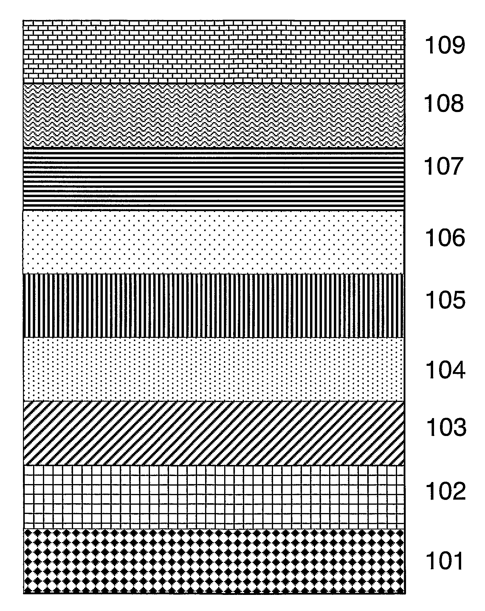
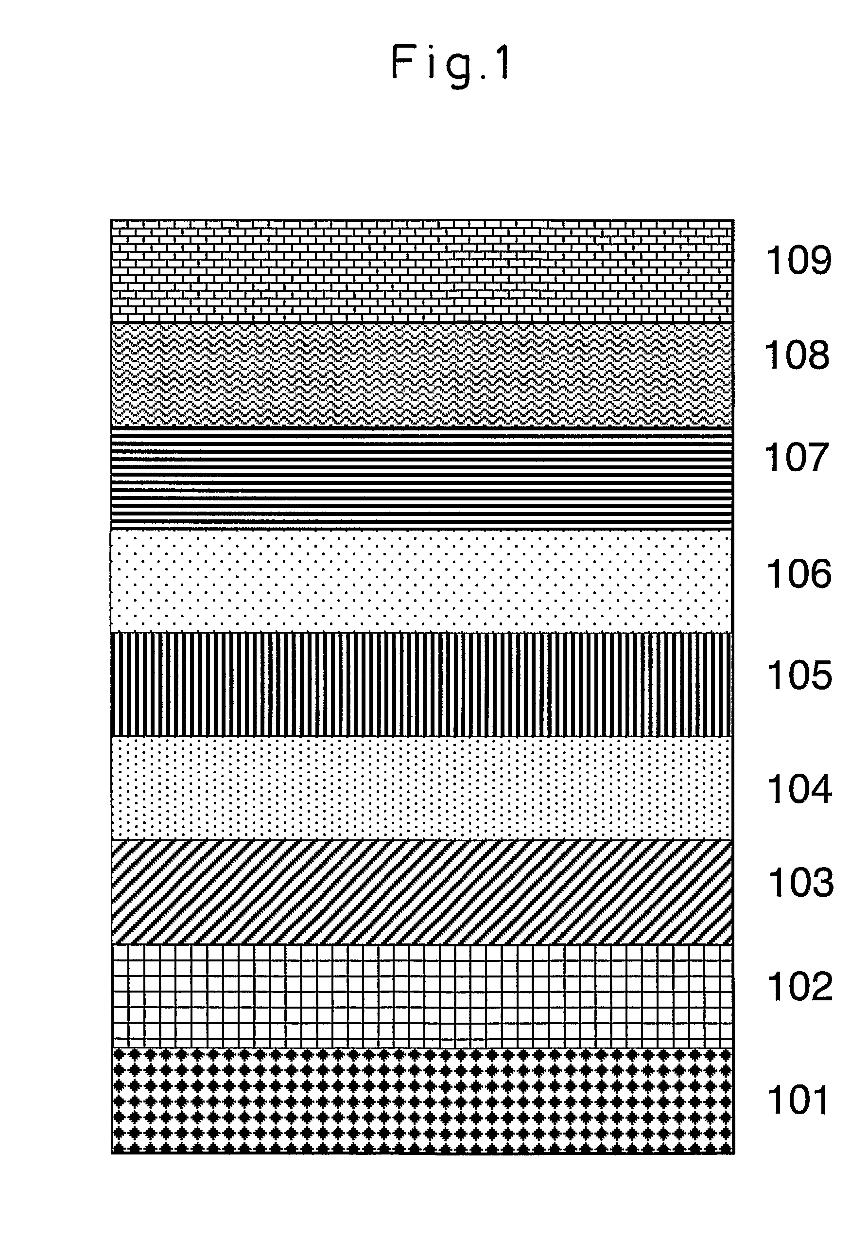
[0086]A light-emitting device was fabricated by using the n-type Group III nitride semiconductor stacked layer structure of the present invention. FIG. 1 is a diagram schematically illustrating the semiconductor stacked structure of a light-emitting device fabricated in this Example. Reference numeral 101 denotes a substrate made of sapphire, 102 denotes a high temperature buffer layer of AlN, and 103 denotes an base layer of undoped GaN. Reference numeral 104 denotes a first n-type layer of Ge-doped GaN, which works as an n-contact layer in the light-emitting device. Reference numeral 105 denotes a second n-type layer of Ge-doped GaN, and 104 and 105 constitute the n-type Group III nitride semiconductor stacked layer structure of the present invention. Reference numeral 106 denotes an n-clad layer of Si-doped InGaN, 107 denotes a light-emitting layer of a multiple quantum well structure, 108 denotes a p-clad layer of Mg-doped AlGaN, and 109 denotes a p-contact layer of Mg-doped AlG...

example 2

[0108]In this Example, a Group III nitride semiconductor light-emitting device was fabricated in the same manner as in Example 1 with the exception of setting the concentrations of impurity atoms in the higher concentration layer and in the lower concentration layer in the second n-type layer 105 to be the same as the concentration of impurity atoms in the first n-type layer 104, decreasing the thickness of the higher concentration layer to be 3 nm, increasing the thickness of the lower concentration layer to be 30 nm, and setting the recurring periodic number of the higher concentration layers and of the lower concentration layers to be 5 times. Therefore, the first n-type layer 104 contained Ge atoms at an average concentration of 6.5×1018 cm−3 which was the same as that of Example 1, and the second n-type layer 105 contained Ge atoms at an average concentration of 2×1018 cm−3.

[0109]The obtained light-emitting device was evaluated in the same manner as in Example 1. The chip exhib...

example 3

[0112]In this Example, a Group III nitride semiconductor light-emitting device was fabricated in the same manner as in Example 1 with the exception of forming the second n-type layer 105 by using a layer homogeneously doped with Ge at a low concentration. In the second n-type layer 105, the amount of doping with Ge was set to be 1 / 25 that of the higher concentration layer in the first n-type layer 104 and the thickness was set to be 0.04 μm. That is, the second n-type layer 105 contained Ge atoms at a concentration of 4.8×1017 cm−3.

[0113]The obtained light-emitting device was evaluated in the same manner as in Example 1. The chip exhibited forward voltage of 3.2 V at a forward current of 20 mA. The emission center wavelength of the band of blue light emission at a forward current of 20 mA was found to be 465 nm. The emission intensity of the light emitted from the chip, as determined through a typical integrating sphere, was 5.2 mW. Thus, a Group III nitride semiconductor light-emit...


PUM

PropertyMeasurementUnit
thicknessesaaaaaaaaaa
thicknessaaaaaaaaaa
thicknessaaaaaaaaaa

Abstract

An n-type Group III nitride semiconductor stacked layer structure including a first n-type layer which includes a layer containing n-type impurity atoms at a high concentration and a layer containing n-type impurity atoms at a low concentration, a second n-type layer containing n-type impurity atoms at an average concentration smaller than that of the first n-type layer, the second n-type layer neighboring the layer containing n-type impurity atoms at a low concentration in the first n-type layer.

Description

CROSS REFERENCE TO RELATED APPLICATION[0001]This application is an application filed under 35 U.S.C. §111(a) claiming benefit, pursuant to 35 U.S.C. §119(e)(1), of the filing date of the Provisional Application No. 60 / 611,285 filed on Sep. 21, 2004, pursuant to 35 U.S.C. §111(b).TECHNICAL FIELD[0002]The present invention relates to an n-type Group III nitride semiconductor stacked layer structure and to a Group III nitride semiconductor light-emitting device including the semiconductor stacked layer structure.BACKGROUND ART[0003]Conventionally, a Group III nitride semiconductor formed on a substrate has been used as a functional material for fabricating pn-junction Group III nitride semiconductor light-emitting devices which emit visible light of short wavelength such as light-emitting diodes (LEDs) and laser diodes (LDs) (see, for example, Japanese Patent Application Laid-Open (kokai) No. 2000-332364). For example, in fabrication of an LED emitting near-UV light, blue light, or gre...

Claims


Application Information

Patent Timeline
Patent Type & Authority Patents(United States)
IPC IPC(8): H01L29/06H01L29/24H01L31/0328H01L31/0336H01L31/072H01L31/109H01L33/00H01L33/06H01L33/32H01L33/36H01L33/50H01L33/56H01L33/62
CPCB82Y20/00H01L29/155H01L33/02H01L33/32H01L29/2003H01L33/025H01L2224/45144H01L2224/73265H01L2224/48257H01L2224/48247H01L2224/48091H01L2224/32245H01S5/34333H01L2924/00014H01L2924/00H01L2924/00012H01L24/73
Inventor TAKEDA, HITOSHIMIKI, HISAYUKI
Owner TOYODA GOSEI CO LTD
Why Eureka
Try Eureka