High fill-factor sensor with reduced coupling

a sensor and high fill-factor technology, applied in the field of digital radiographic imaging, can solve the problems of increasing signal coupling between data and switching electrodes, relatively poor fill-factor of sensor devices, increasing thermal or “dark state” noise, etc., to achieve high fill-factor, reduce thermal noise and capacitive coupling, and improve data isolation

Inactive Publication Date: 2009-11-10
CARESTREAM HEALTH INC
View PDF36 Cites 22 Cited by
  • Summary
  • Abstract
  • Description
  • Claims
  • Application Information

AI Technical Summary

Benefits of technology

[0024]It is an advantage of the present invention that it provides a photosensor array having a high fill factor and having reduced thermal noise and capacitive coupling.
[0025]It is a feature of the present invention that it provides improved isolation of data, gate switching, and bias electrodes. The arrangement of the present invention provides significantly reduced coupling when using a conductive substrate. The apparatus of the present invention allows the use of a data line having lower resistance for improved conductivity, resulting in reduced thermal noise. The thick insulator between the front and back planes and the gate dielectric layer helps to reduce capacitive coupling and cross-talk, as well as helps to minimize the possibilities of shorts between conductive layers.

Problems solved by technology

As a result, the sensor device suffers from relatively poor fill-factor and is able to use only a fractional portion of the light emitted from the phosphor screen.
However, with more compact packaging comes the complication of increased signal coupling between data and switching electrodes and increased thermal or “dark state” noise due to Johnson noise effects.
The capacitive coupling problem becomes even more acute when the imaging array is formed on a conductive stainless steel substrate.
However, capacitive coupling effects can compromise the overall performance of a plate formed on a stainless steel substrate.
The conductive materials that are conventionally used for making connections to array sensing electronics are not ideal conductors and must be selected from among a somewhat limited group of materials.
Aluminum, although a better conductor, exhibits a tendency to diffuse into silicon and to form hillock- and whisker-type defects at high temperatures, rendering it an unsuitable alternative for many semiconductor designs.
However, current fabrication techniques typically form these metal electrode structures on the backplane with a thin a-SiN:H dielectric separation layer that is typically only a few hundred nanometers thick, resulting in generally higher coupling, higher crosstalk levels.
This could also result in increasing the likelihood of interlayer shorts manufacturing defects.

Method used


Image

  • High fill-factor sensor with reduced coupling
  • High fill-factor sensor with reduced coupling
  • High fill-factor sensor with reduced coupling

Examples


Embodiment Construction

[0041]The present description is directed in particular to elements forming part of, or cooperating more directly with, apparatus in accordance with the invention. It is to be understood that elements not specifically shown or described may take various forms well known to those skilled in the art.

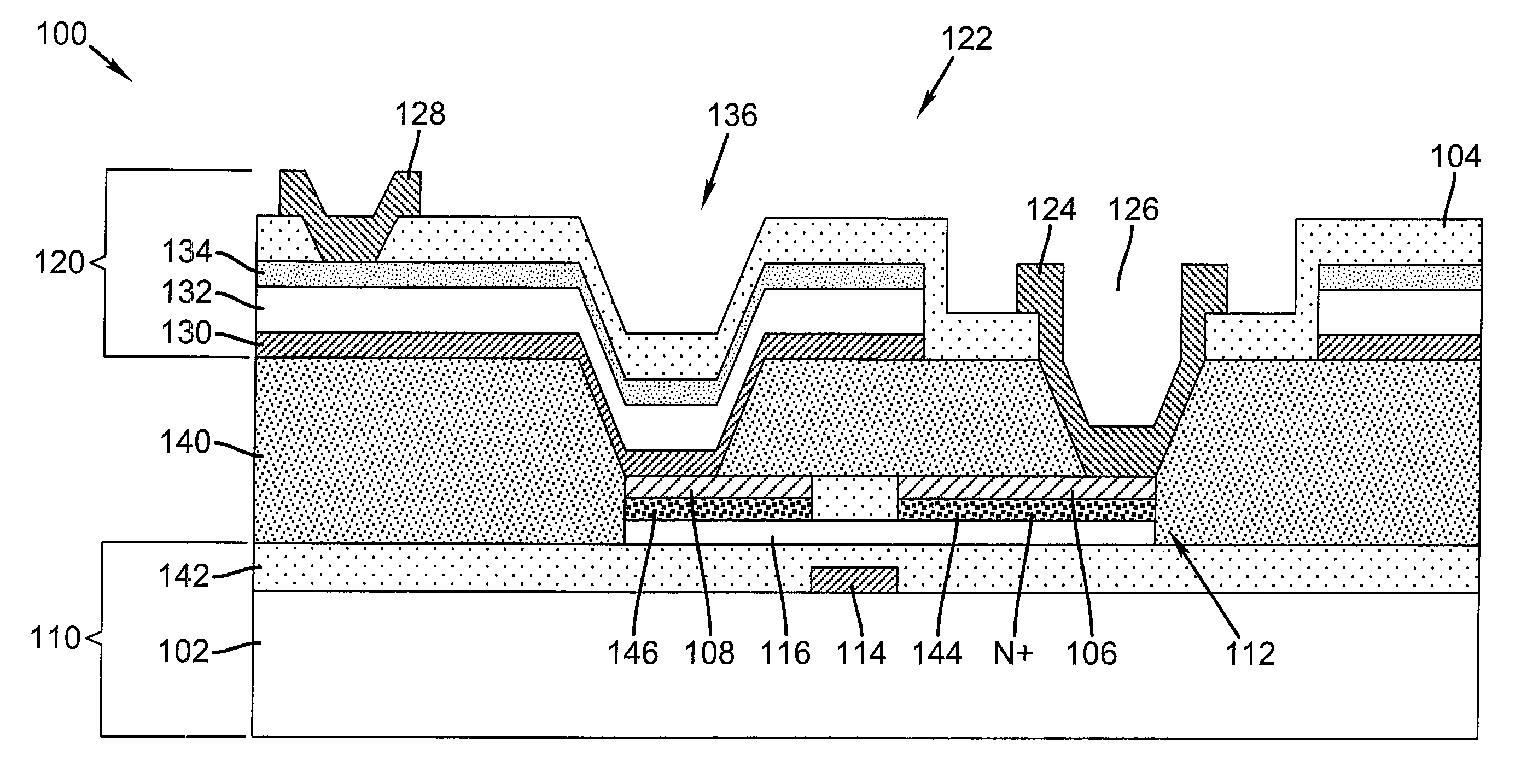
[0042]Referring to FIG. 2, there is shown a cross-sectional view of a pixel sensing circuit 100 according to an embodiment of the present invention. A substrate 102 on which circuit 100 is formed can be glass, plastic, or an inorganic film, polyimide, acrylic resin, benzocyclobutene (BCB), or the like or some other material, including stainless steel, for example, coated with a dielectric, such as BCB or spin-on glass. Electronic components and sensors are fabricated as part of a backplane 110 or a front plane 120. An insulating layer 140 separates backplane 110 from front plane 120. Insulating layer 140 can be, for example, benzocyclobutene (BCB), polyimide, sol-gel, acrylic, or some othe...


PUM


Abstract

A photosensor array includes data and scan lines (124, 148), circuitry of each data line / scan line pair formed in a backplane (110) on a substrate (102). On a first electrode scan line (148) a switching element (112) responds to a scan signal, connecting a first terminal (106) to a second terminal (108). A front plane (120) has sensing elements (122) indicating a measure of a received stimulus and including a charge collection electrode (130). An insulating layer (140) disposed between the backplane (110) and the front plane (120) contains at least a first via (136) connecting the first terminal (108) of the switching element (112) in the backplane (110) to a charge collection electrode (130) of the sensing element (122) in the front plane (120). A second via (126) connects between the second terminal (108) of the switching element (112) and the data line (124).

Description

FIELD OF THE INVENTION[0001]This invention generally relates to digital radiographic imaging and more particularly relates to an imaging array having an improved fill factor and reduced capacitive coupling between data electrodes and conductive structures.BACKGROUND OF THE INVENTION[0002]A digital radiography imaging panel acquires image data from a scintillating medium using an array of individual sensors, arranged in a row-by-column matrix so that each sensor provides a single pixel of image data.[0003]For these devices, hydrogenated amorphous silicon (a-Si:H) is commonly used to form the photodiode and the thin-film transistor (TFT) switch. FIG. 1A shows a cross-section (not to scale) of a single imaging pixel 10 in a prior art a-Si:H based flat panel imager. Each imaging pixel 10 has, as shown in FIG. 1B, a photodiode 70 and a TFT switch 71.[0004]A layer of X-ray converter material (e.g., luminescent phosphor screen 12), shown in FIG. 1, is coupled to the photodiode-TFT array. P...

Claims


Application Information

Patent Timeline
Patent Type & Authority Patents(United States)
IPC IPC(8): H01L31/00
CPCH01L27/14658H01L27/146
Inventor HEILER, GREGORY N.TREDWELL, TIMOTHY J.BEDZYK, MARK D.KERR, ROGER S.VYGRANENKO, YURIYSTRIAKHILEV, DENISHONG, YONGTAEKLAI, JACKSON C. S.NATHAN, AROKIA
Owner CARESTREAM HEALTH INC
Why Eureka
Try Eureka