Organic light emitting display apparatus

a light-emitting display and organic technology, applied in the direction of organic semiconductor devices, thermoelectric devices, solid-state devices, etc., can solve the problems of oxidizing the layer itself, limiting the aperture ratio, and reducing the light-emitting voltag

Active Publication Date: 2009-11-17
SAMSUNG DISPLAY CO LTD +1
View PDF10 Cites 11 Cited by
  • Summary
  • Abstract
  • Description
  • Claims
  • Application Information

AI Technical Summary

Problems solved by technology

However, in the organic light emitting display apparatus of the structure in which the emitted light is taken out from the back side (substrate side), in case of using an active matrix which has the advantages of higher definition and larger display size over a simple matrix, the aperture ratio is subject to limitation.
In the top emission type organic light emitting element, the layer interposed between the upper electrode and the organic layer needs to be reduced in thickness because of the problem of low transmittance or low conductivity, and it is impossible to prevent the organic layer from being oxidized when the upper electrode is formed, giving rise to the problem of elevated light emission voltage.
According to Patent Document 1 mentioned above, although it is possible to protect the organic buffer layer from being damaged during high energy deposition, the buffer layer itself is oxidized when the upper electrode is formed, and the rise of light emission voltage is unavoidable.

Method used


Image

  • Organic light emitting display apparatus
  • Organic light emitting display apparatus
  • Organic light emitting display apparatus

Examples


example 1

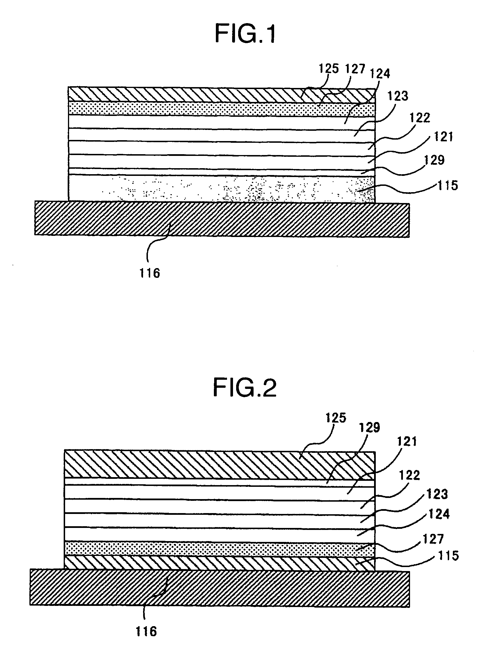
[0061]An example of organic light emitting display apparatus according to the present invention is explained below. FIG. 1 is a cross-sectional view of the organic light emitting display apparatus according to Example 1 of the present invention. The lower electrode 115 comprises an Cr film formed by EB deposition. The electrode film was patterned by using a shadow mask, and its thickness was 100 nm.

[0062]Then a 50 nm thick co-deposition film of F4-TCNQ and copper phthalocyanine was formed by two-source simultaneous vacuum deposition using a shadow mask for patterning. The F4-TCNQ:copper phthalocyanine molar ratio was 1:1. This co-deposition film functions as a hole injection layer 129.

[0063]Then a film of 4,4-bis[N-(1-naphthyl)-N-phenylamino]biphenyl (hereinafter abbreviated as α-NPD) with a thickness of 50 nm was formed by vacuum deposition using a shadow mask for patterning. The deposition region was 1.2 times each edge of the lower electrode. This α-NPD film works as a hole trans...

example 2

[0071]Another example of organic light emitting display apparatus of the present invention is explained below.

[0072]An organic light emitting display apparatus same as Example 1 in structure but different in thickness of the buffer layer was fabricated.

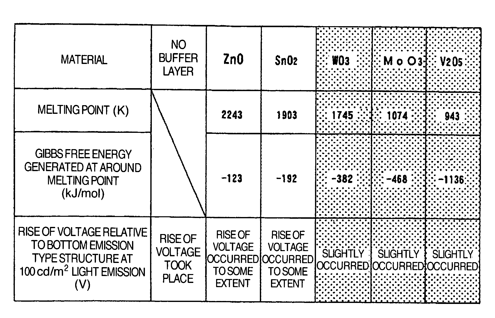
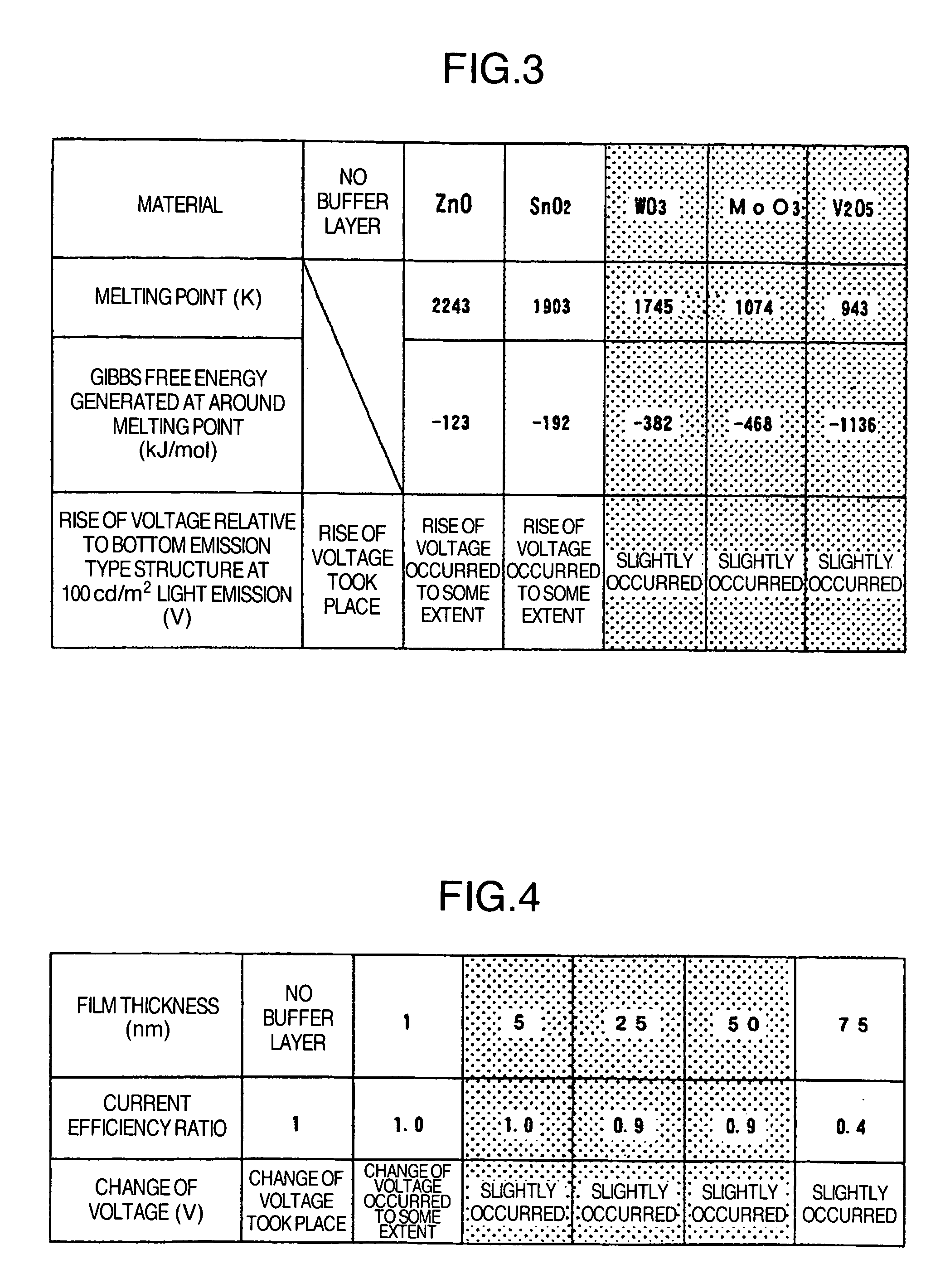
[0073]A film of vanadium oxide was formed as buffer layer 127 by EB deposition using a shadow mask for patterning. The film thickness was 1, 5, 25, 50 and 75 nm. A similar display apparatus having no buffer layer was also made by way of comparison. The vanadium oxide film had a composition of V:O=1:2.45.

[0074]FIG. 4 shows the change of voltage and current efficiency ratio according to the buffer layer thickness at 100 cd / m2 light emission. The change of voltage shown here is the one relative to the bottom emission type display apparatus shown in FIG. 2. Current efficiency ratio is the ratio to the current efficiency of the bottom emission type display apparatus which is supposed to be 1. If the buffer layer thickness is less than 5 nm...

example 3

[0075]Still another example of the organic light emitting display apparatus according to the present invention will be explained. FIG. 5 is a cross-sectional view of the organic light emitting display apparatus in the instant example of the present invention.

[0076]A 150 nm thick Al—Si film was formed by sputtering as reflection electrode 200 and patterned by photolithography. Also, an ITO film, 90 nm thick, was formed by sputtering as lower electrode 115 and patterned by photolithography.

[0077]Then polyethylenedioxythiophene (PEDT) incorporated with polystyrenesulfonic acid (PSS) was spin coated thereon to form a film having a thickness of 40 nm after dried at 200° C. This PSS-incorporated PEDT film functions as a hole injection layer 129.

[0078]On this film was further spin coated polyfluorene to form a 40 nm thick film after dried at 80° C. This polyfluorene film serves as a light emitting layer 122.

[0079]On this polyfluorene film was formed an Alq film, 10 nm thick, by vacuum depo...


PUM


Abstract

The present invention provides a top emission type organic light emitting display apparatus in which manufacture it is possible to prevent the organic film from being oxidized when the upper transparent electrode is formed, and which is capable of emitting light at a low voltage. This organic light emitting display apparatus includes an organic light emitting layer and an upper electrode and a lower electrode sandwiching the said organic light emitting layer between them, and is of a structure in which the light emitted from the organic light emitting layer is taken out from the upper electrode side, wherein a buffer layer mostly made of an oxide with its Gibbs free energy generated at around the melting point being lower than −300 kJ / mol is provided between the organic light emitting layer and the upper electrode, the side of the organic layer which is in contact with the buffer layer being doped with an electron donative dopant.

Description

BACKGROUND OF THE INVENTION[0001]The present invention relates to an organic light emitting display apparatus.[0002]Recently, attention has been focused on the organic light emitting display apparatus as the next generation flat panel displays. Such organic light emitting display apparatus have outstanding advantageous properties such as spontaneous light emission, wide visual field and angle, and high response speed.[0003]The conventional organic light emitting elements are of a structure comprising, laminated on a glass substrate, a first electrode made of ITO or the like, an organic layer comprising a hole transport layer, a light emitting layer and an electron transport layer, and an upper electrode of a low work function. The emitted light passes through the first electrode which is transparent, and is taken out from the back side (substrate side) of the structure.[0004]However, in the organic light emitting display apparatus of the structure in which the emitted light is taken...

Claims


Application Information

Patent Timeline
Patent Type & Authority Patents(United States)
IPC IPC(8): H01L35/24H01L51/00
CPCH01L51/5221H01L51/5048H01L2251/5315H10K50/14H10K2102/3026H10K59/80524H10K50/828
Inventor MURAKAMI, HAJIMESHIMIZU, MASAOARATANI, SUKEKAZUTANAKA, MASAHIRO
Owner SAMSUNG DISPLAY CO LTD
Why Eureka
Try Eureka