Manufacturing method of semiconductor device

a manufacturing method and semiconductor technology, applied in the field of manufacturing methods of semiconductor devices, can solve the problems of difficult formation of micropatterns through lithography process, and achieve the effects of reducing the distance between adjacent gates (gate pitch), significantly improving the degree of integration of the integrated circuit, and improving the degree of integration

Inactive Publication Date: 2009-11-24
SEMICON ENERGY LAB CO LTD
View PDF22 Cites 6 Cited by
  • Summary
  • Abstract
  • Description
  • Claims
  • Application Information

AI Technical Summary

Benefits of technology

[0009]It is said that the unit cost of IC cards or IC tags has to be reduced to 10 yen or less in order to promote the use of IC cards or IC tags throughout society. In order to reduce the unit cost of IC cards or IC tags, it is necessary to achieve high integration of an IC chip that is an essential component of the IC cards or IC tags and to reduce a chip area so that the number of chips that can be obtained from one substrate can be increased. In addition, the productivity of IC chips has to be improved by using a large-area glass substrate. However, since a thin glass substrate is slightly curved in the micro level, it has been difficult to form micropatterns through a lithography process which transfers patterns of a photomask.
[0010]In view of the foregoing, it is an object of the invention to provide a manufacturing method of a semiconductor device with a reduced chip area by reducing the size of a pattern for forming an integrated circuit. For example, the invention can reduce the size of an IC chip which includes thin film transistors and is provided as an application of IC cards or IC tags.
[0013]In the invention, a phase-shift lithography method is used to form a pattern of a contact hole (specifically, a contact hole for connecting a semiconductor layer to a wiring layer) or a gate electrode, by which the degree of integration of an integrated circuit can be significantly improved. Accordingly, micropatterns can be formed in a wide area even over a substrate with low planarity such as a glass substrate.
[0014]That is, the degree of integration can be improved by forming patterns of wirings, contact holes, and the like that are necessary for an integrated circuit by use of a phase-shift lithography method or a holographic lithography method, within the resolution limit of lithography.
[0015]In the case of opening a contact hole, a contact area located under the contact hole can be designed with a smaller margin. That is, a redundant area which can accommodate a misalignment of a contact hole can be reduced.
[0016]In the case of a pattern such as a memory cell array in which transistors are periodically arranged, the distance between adjacent gates (gate pitch) can be reduced.

Problems solved by technology

However, since a thin glass substrate is slightly curved in the micro level, it has been difficult to form micropatterns through a lithography process which transfers patterns of a photomask.

Method used


Image

  • Manufacturing method of semiconductor device
  • Manufacturing method of semiconductor device
  • Manufacturing method of semiconductor device

Examples


embodiment mode 1

[0072]A manufacturing method of a semiconductor device using the above-described lithography technique which is capable of micropattern formation is described with reference to the drawings. In the following description, a static random access memory (SRAM) having six transistors is illustrated as an example of a memory cell.

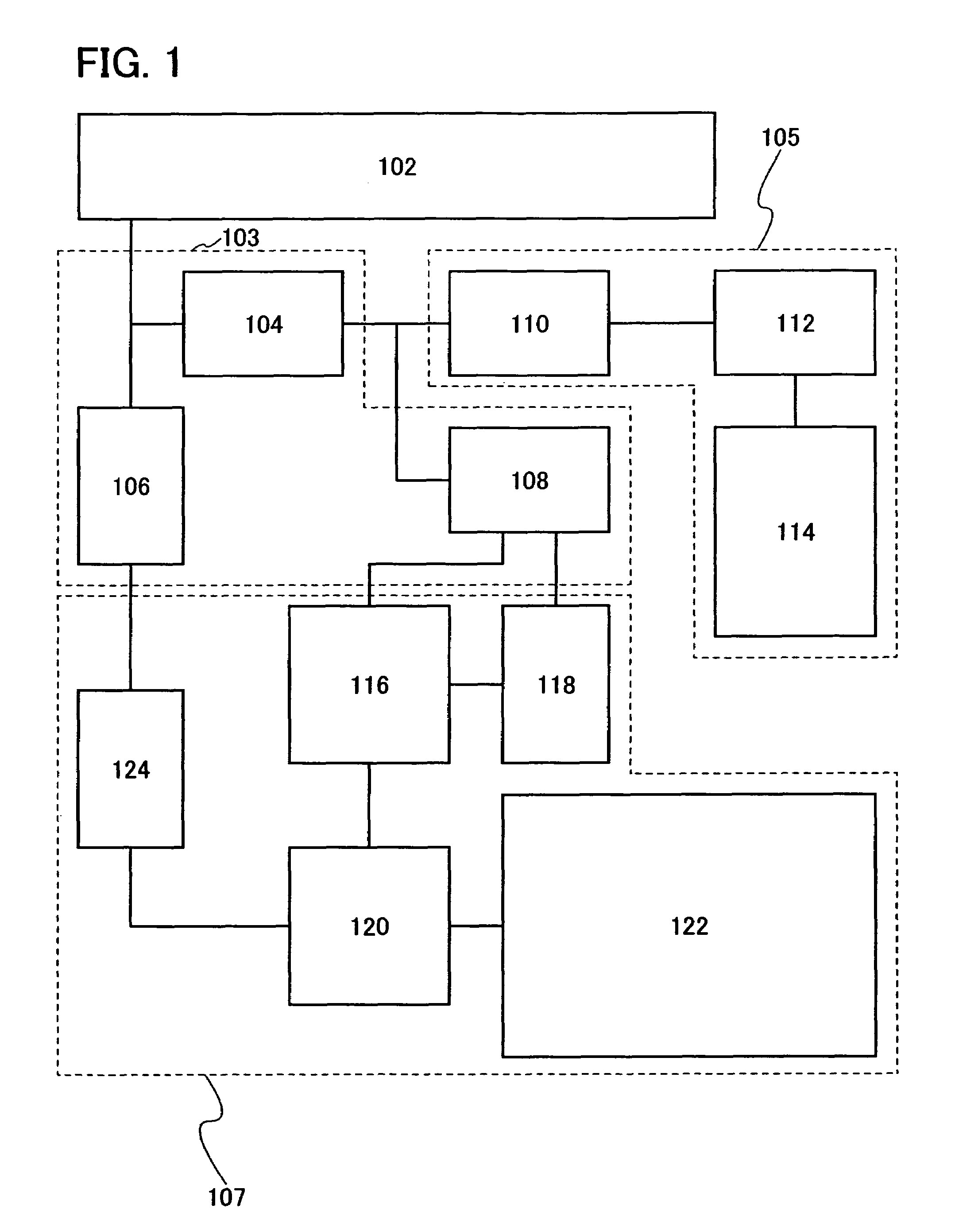
[0073]Inputs of inverters 301 and 302 in this SRAM are connected to bit lines BL1 and BL2 through switches S1 and S2, respectively. The switches S1 and S2 are controlled by a row selection signal which is delivered through a word line WL. Each of the inverters 301 and 302 is supplied with power from a high voltage VDD and a low voltage GND which is generally grounded. In order to write data into the memory cell, the voltage VDD is applied to one of the bit lines BL1 and BL2, while the voltage GND is applied to the other of the bit lines BL1 and BL2.

[0074]The inverter 301 includes an n-channel transistor N1 and a p-channel transistor P1 which are connected in ser...

embodiment mode 2

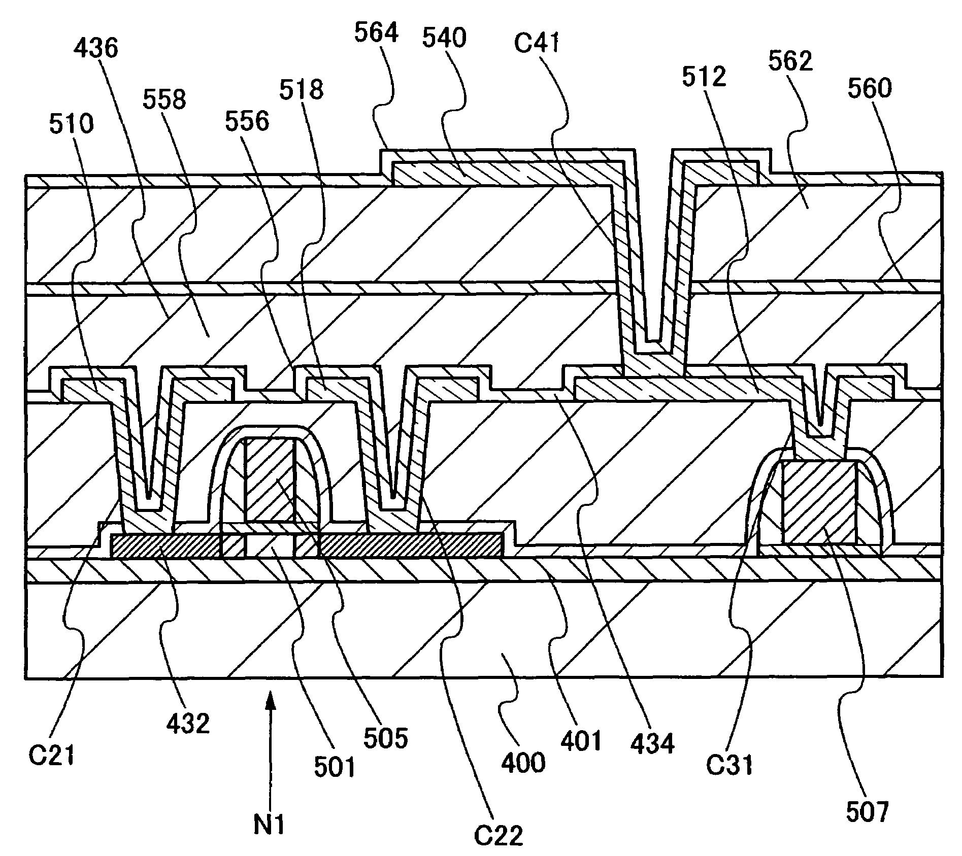
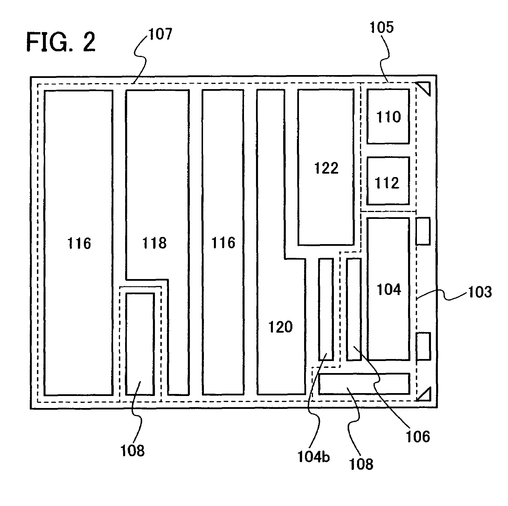
[0094]FIG. 11 shows another example of a circuit layout of the SRAM shown in FIG. 5. FIG. 11 shows an SRAM having a semiconductor layer, a gate electrode layer, and three wiring layers. The SRAM includes semiconductor layers 501 and 502 for forming n-channel transistors, and semiconductor layers 503 and 504 for forming p-channel transistors. Further, gate electrode layers 505, 506, 507, and 508 functioning as gate wiring layers are provided over the semiconductor layers 501, 502, 503, and 504 with an insulating layer interposed therebetween. Thus, the n-channel transistors N1 and N2, the p-channel transistors P1 and P2, and the switches S1 and S2 are formed.

[0095]First wiring layers 510, 512, 514, 516, 518, 520, 522, 524, 526, and 528 which contact the gate electrode layers are provided over a first interlayer insulating layer. Second wiring layers 532 and 536 for forming bit lines and second wiring layers 530 and 538 for forming ground potential lines are provided over a second int...

embodiment mode 3

[0108]Instead of performing the phase-shift lithography illustrated in Embodiment Modes 1 and 2, holographic lithography can be performed. By using holographic lithography for formation of gate electrodes and / or contact holes, miniaturization of transistors can be achieved as well as a gate pitch (intervals between contact holes) can be narrowed.

[0109]In that case, it is possible to use a holographic lithography technique for formation of gate electrodes and use a lithography process with a phase-shift mask for formation of contact holes. While the holographic lithography can form micropatterns, it involves a large number of masks and high cost. The same can be said for a computer-generated hologram mask. On the other hand, by combining the holographic lithography technique with the lithography process using the phase-shift mask, it becomes possible to minimize the increase of mask cost and decrease of throughput. Therefore, formation of micropatterns and high productivity can be en...


PUM


Abstract

To provide a manufacturing method of a semiconductor device with a reduced chip area by reducing the size of a pattern for forming an integrated circuit. For example, the size of an IC chip that is provided as an application of IC cards or IC tags can be reduced. The manufacturing method includes the steps of forming a gate electrode; forming an insulating layer over the gate electrode; and forming an opening in the insulating layer. One or both of the step of forming the gate electrode and the step of forming the opening in the insulating layer is / are conducted by a lithography process using a phase-shift mask or a hologram mask. Accordingly, micropatterns can be formed even over a substrate with low planarity such as a glass substrate.

Description

BACKGROUND OF THE INVENTION[0001]1. Field of the Invention[0002]The present invention relates to a manufacturing method of a semiconductor device having an integrated circuit which includes transistors formed over an insulating surface. In particular, the invention relates to a manufacturing method of a semiconductor device using a high-resolution lithography technique.[0003]2. Description of the Related Art[0004]As a semiconductor device which performs transmission / reception of instructions or data with radio signals, a semiconductor device which includes an integrated circuit having thin film transistors (hereinafter also referred to as “TFTs”) formed over a glass substrate as well as an antenna attached thereto is known (for example, see Reference 1: Japanese Published Patent Application No. 2005-202947).[0005]Such a semiconductor device is called an IC card or an IC tag depending on the use or modes, and is planned to be used for identification of goods or individuals. That is, ...

Claims


Application Information

Patent Timeline
Patent Type & Authority Patents(United States)
IPC IPC(8): H01L21/00H01L21/44H01L21/84
CPCH01L21/266H01L21/76816H01L21/84H01L23/5227H01L27/1214H01L27/1288H01L2924/0002H01L2924/00
Inventor OHNUMA, HIDETO
Owner SEMICON ENERGY LAB CO LTD
Why Eureka
Try Eureka