Method of fabricating semiconductor device including forming a protective layer and removing after etching a trench

a technology of etching and trench bottom, which is applied in the manufacture of microstructural devices, microstructures, electrical equipment, etc., can solve the problems of difficult to obtain sufficient ions with the etched surface, difficult to remove the etching obstruction layer at the trench bottom, and inapplicability of the fine etching technology used in recent years to fabricate semiconductors. achieve the effect of improving the detachment of the polymer film

Inactive Publication Date: 2009-11-24
LAPIS SEMICON CO LTD
View PDF12 Cites 20 Cited by
  • Summary
  • Abstract
  • Description
  • Claims
  • Application Information

AI Technical Summary

Benefits of technology

[0033]The present invention can improve the detachment of the polymer film from the trench side walls by conducting the heat treatment within a temperature range of 300 to 500° C., for example, after the trench etching and before plasma ashing treatment.

Problems solved by technology

Therefore, the fine etching technology (in particular, the dry etching technology) that has been used to fabricate the semiconductors in recent years are often not applicable as is as the MEMS structure etching technology.
However, in the bottom of a trench with a width of several tens of μm and a depth of several hundred μm as required by the MEMS structure, it is hard to obtain the bombardment of sufficient ions with the etched surface for the above reasons and, as a result, the etching obstruction layer at the trench bottom cannot be adequately removed and, ultimately, the etching stops when a certain depth is reached.
Also, the total etching time is extremely long so that the mask material retreats during the etching and there is no mask material before the desired trench shape is obtained.
In other words, this is because it is difficult to increase the mask selectivity.
Thus, even when the pattern has a high aspect ratio, the balance between the trench bottom etching and film deposition does not readily collapse and, hence, the etching stop does not readily occur.
In particular, when the deposited film adheres on a moving part of the MEMS structure, a serious problem (i.e., operational defect) is produced.
However, when the trench side walls undergo the deep trench etching using the ICP plasma etching apparatus, the deposited fluorocarbon plasma polymer film cannot be completely removed in the plasma ashing.
The inventor thought that the C4F8 gas is highly dissociated in the plasma so that a film containing a large number of C—C bonds with a strong associative strength are formed and, as a result, detachment of the film becomes difficult.

Method used


Image

  • Method of fabricating semiconductor device including forming a protective layer and removing after etching a trench
  • Method of fabricating semiconductor device including forming a protective layer and removing after etching a trench
  • Method of fabricating semiconductor device including forming a protective layer and removing after etching a trench

Examples


first embodiment

[0039]The method of fabricating a MEMS device according to the first embodiment of the present invention is characterized in that, directly after the silicon trench etching, heating is performed within a temperature range of 300 to 500° C. followed by oxide plasma ashing to remove the fluorocarbon plasma polymer film deposited on the trench side walls.

[0040][A] Trench Etching

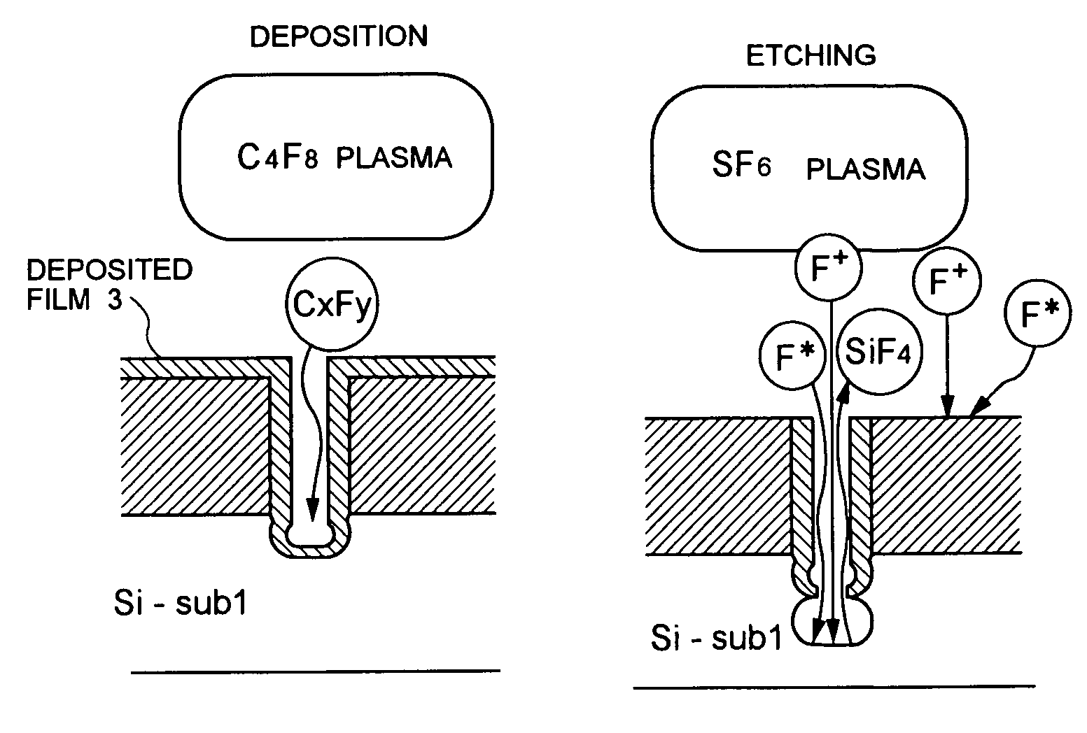
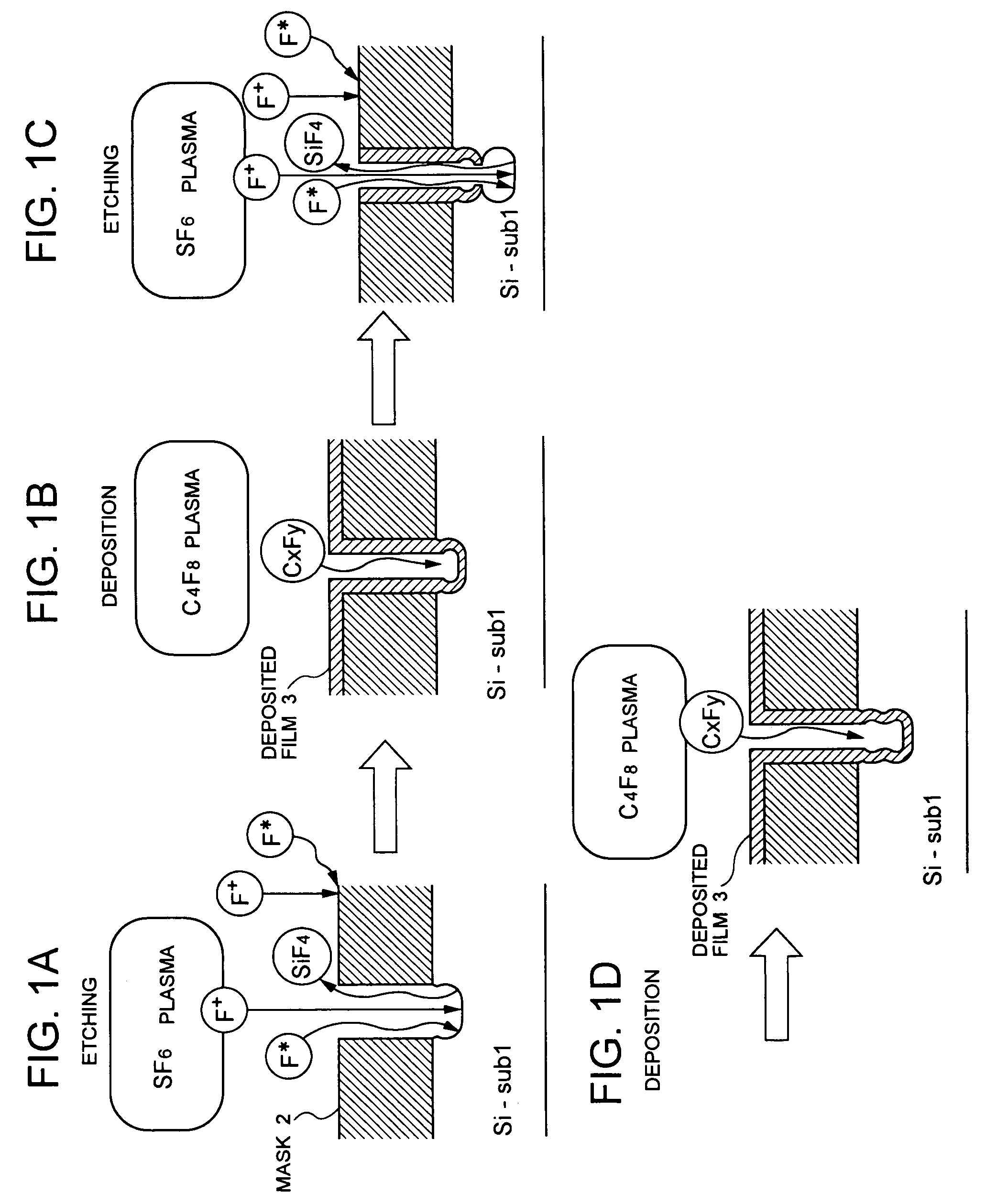
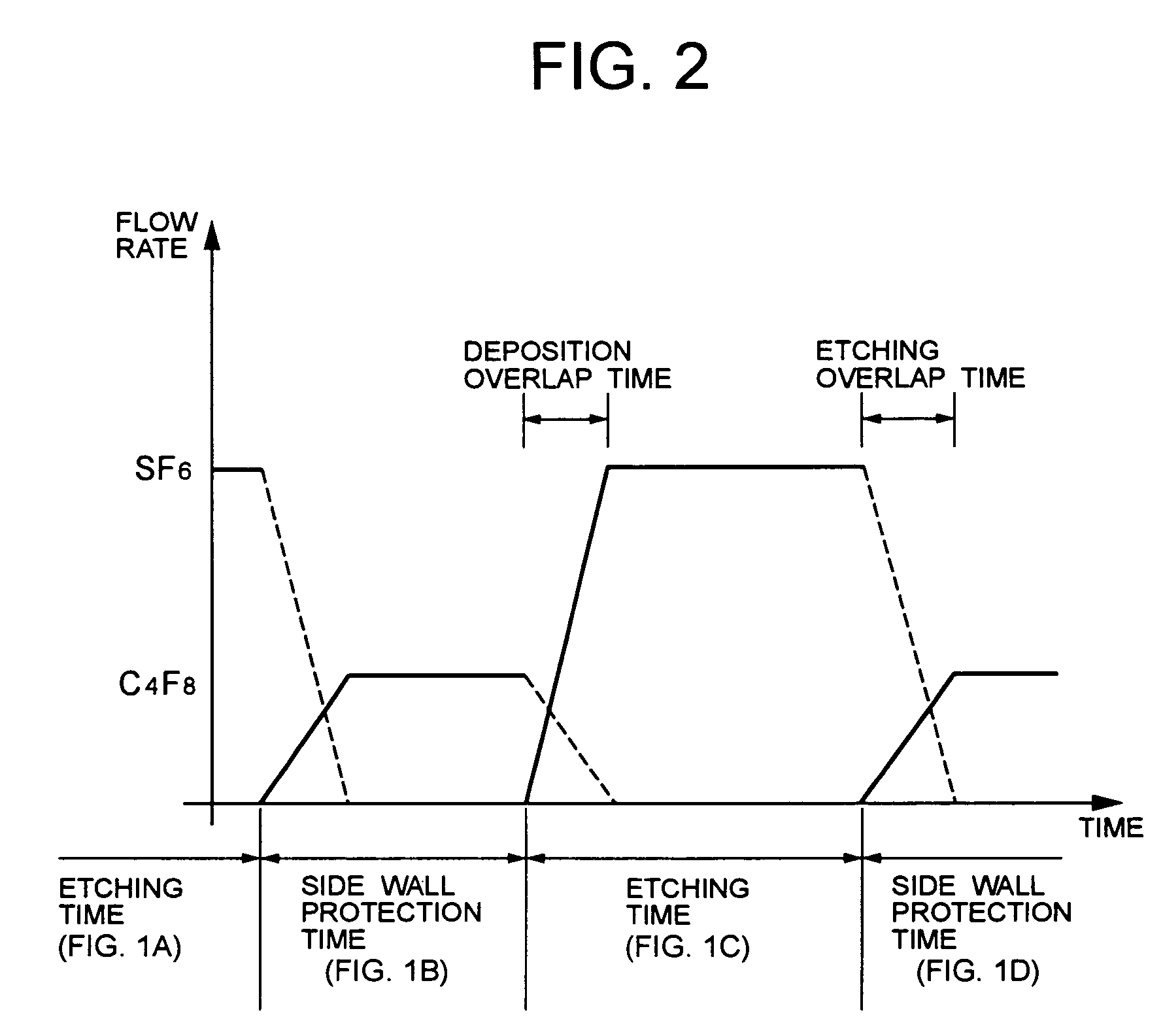
[0041]FIG. 1A to FIG. 1D are a series of diagrams to illustrate a sequence of the silicon trench etching of the first embodiment of the present invention. In the first embodiment (FIG. 1A to FIG. 1D), trench etching of silicon 1 is performed by alternately repeating a silicon etching step (FIGS. 1A and 1C) and a deposition step (FIG. 1B and FIG. 1D). The silicon (Si-sub) 1 is a semiconductor substrate (wafer). The silicon etching step includes forming a photoresist etching mask 2 on the silicon 1, and etching the silicon with F radicals (F*) and F+ ions generated by SF6 gas plasma. The deposition step includes d...

experiment 1

Deposition of Polymer Film

[0053]One silicon sample was prepared by cleaving a silicon wafer. The silicon sample was a 10 mm×10 mm piece. The ICP-plasma deposition step was conducted such that C4F8 plasma was irradiated for one minute onto the surface of the silicon wafer to deposit a fluorocarbon polymer film onto the silicon wafer surface. Thus, the fluorocarbon polymer film deposited on the pattern side walls was reproduced in simulated fashion.

experiment 2

Heating

[0054]Thereafter, the cleaved silicon sample on which the fluorocarbon polymer film had been deposited was introduced into a chamber of an ultrahigh vacuum (degree of vacuum is 1×10⁻⁹ Torr) thermal desorption spectroscopy (TDS) apparatus that was equipped with a quadrupole mass spectroscopy (QMS) apparatus. The silicon sample was heated to one of four maximum temperatures from room temperature (20° C.) at a rising temperature speed of 1° C. / sec, by irradiating the silicon sample with infrared rays from the outside. The four maximum temperatures were 180° C., 340° C., 500° C. and 700° C. It should be noted that the single sample was used in five different ways. First, the sample was not heated, i.e., it was maintained at 20° C., and the surface of this sample was investigated. The investigation (i.e., observation of the sample surface after heating) will be described in the Experiment 3. Second, the same sample was heated to 180° C., and the sample surface was investigated. Th...


PUM


Abstract

The method of fabricating a semiconductor device includes subjecting a semiconductor substrate to trench etching by alternately repeating an etching step and a deposition step. The etching step creates a trench structure by dry-etching the exposed surface of the semiconductor substrate. An etching mask is formed on the surface of the semiconductor substrate so that the semiconductor substrate has the exposed portion. The deposition step deposits a protection film for suppressing etching of the trench side walls. The method of fabricating a semiconductor device also includes subjecting the semiconductor substrate that has just undergone the trench etching to a heat treatment at a predetermined temperature. The semiconductor substrate is heat-treated within a temperature range of 300 to 500° C. immediately following the trench etching, for example. Plasma ashing is then performed.

Description

BACKGROUND OF THE INVENTION[0001]1. Field of the Invention[0002]The present invention relates to a method of fabricating a semiconductor device such as a MEMS (Micro Electrical Mechanical System) device or MIST (Micro System Technology) device and, more particularly, to a trench side wall treatment following deep trench etching that employs a dry etching technology for forming a three-dimensional structure in a semiconductor substrate.[0003]2. Description of the Related Art[0004]In recent years, attention has been focused on microetching that utilizes semiconductor fine etching technologies to fabricate very minute structures of sizes on the order of a few 100 μm. The application of such minute structures in various sensors and in optical switches and high frequency (RF) products and so forth in the optical communication field has been studied.[0005]Generally, because such microetching-applied products are fabricated using Si processes, these products can be integrated on a chip wit...

Claims


Application Information

Patent Timeline
Patent Type & Authority Patents(United States)
IPC IPC(8): H01L21/31H01L21/302H01L21/461
CPCB81C1/00063H01L21/30655H01L21/02057H04B1/3833
Inventor IKEGAMI, NAOKATSU
Owner LAPIS SEMICON CO LTD
Why Eureka
Try Eureka