
Nanoelectrode array for electrochemical analysis

Active Publication Date: 2009-12-01
NAT TECH & ENG SOLUTIONS OF SANDIA LLC
View PDF1 Cites 20 Cited by
  • Summary
  • Abstract
  • Description
  • Claims
  • Application Information

AI Technical Summary

Benefits of technology

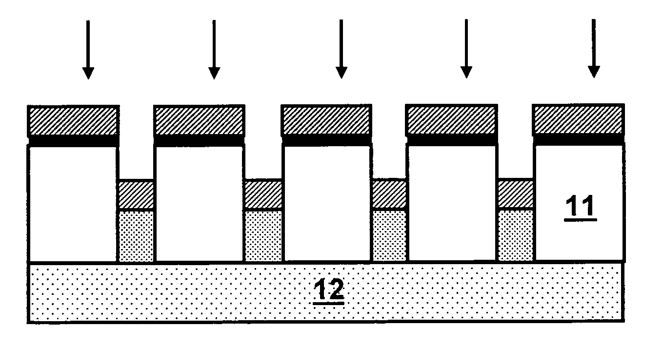
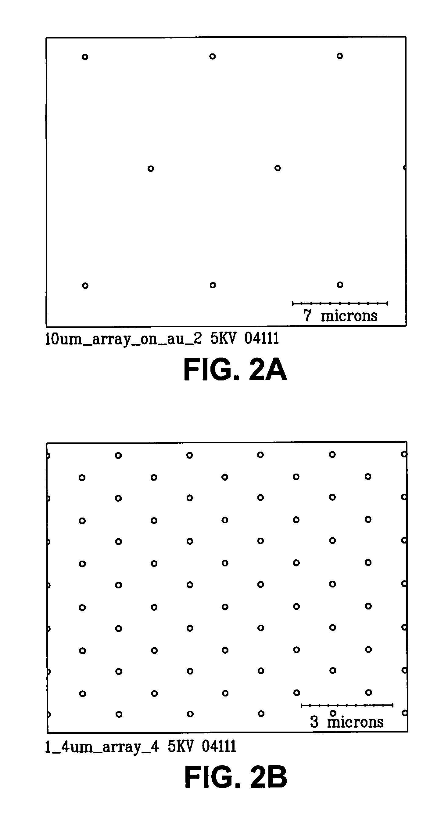
[0006]The present invention is directed to a nanoelectrode array, comprising an electrically conducting substrate, an insulating layer on the substrate, and a plurality of hollow pores formed through the insulating layer to provide a plurality of working nanoelectrodes, wherein each working nanoelectrode has a critical dimension and the plurality of working electrodes has a uniform inter-electrode spacing between each working nanoelectrode. The nanoelect

Problems solved by technology

Unfortunately, electrochemical analysis has historically required that field samples be transported to an analytical laboratory where additional laboratory chemicals must be added to the samples before an electrochemical analysis can be performed with bench-scale equipment.
This requires skilled laboratory technicians and causes unacceptable time delays when immediate information about the safety of a particular water source is needed.
Furthermore, sample degradation may occur during sample transport to the laboratory, thereby causing further uncertainty in the analytical results.
Conventional off-site laboratory analysis is also too costly if comprehensive, continuous monitoring of the health of a water distribution system is desired.
Unfortunately, the incorporation of microelectrodes in analytical methods is severely hampered by the small faradaic currents (i.e., small analytical signals) typical for these electrodes.
However, because the faradaic current from an individual nanoelectrode is very small, a massive array of nanoelectrodes is required to obtain an adequate current signal.
Such integrated nanoelectrode arrays are not readily available using current fabrication techniques.

Method used


Image

  • Nanoelectrode array for electrochemical analysis
  • Nanoelectrode array for electrochemical analysis
  • Nanoelectrode array for electrochemical analysis

Examples


Embodiment Construction

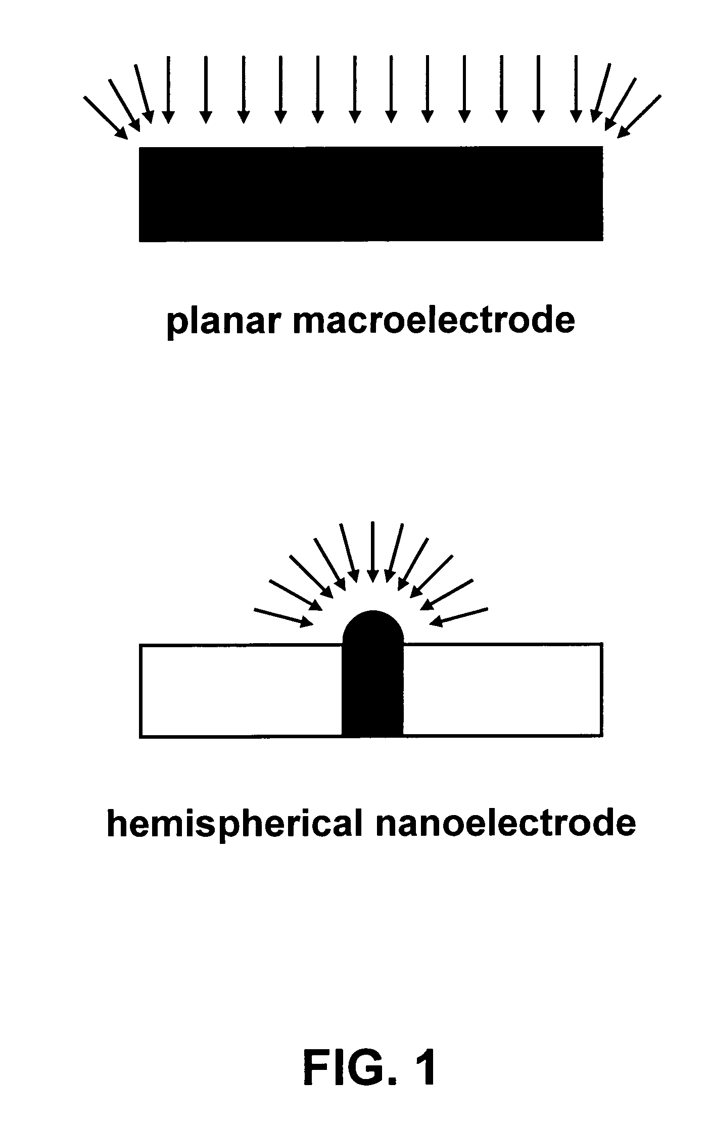
[0015]Shown in FIG. 1 is electrochemical diffusion to a planar macroelectrode. In general, the sensitivity of an electrochemical planar electrode is proportional to the diffusion-limited current density id after application of a step potential, according to

[0016]id=nFDCδ⁢⁢such⁢⁢that⁢⁢δ=(π⁢⁢Dt)1⁢ / ⁢2(1)

where n represents the number of electrons transferred in the electrochemical reaction, F is Faraday's constant, D is the diffusion coefficient of the electroactive species, C is the bulk concentration of the species in the solution far from the electrode, and δ is the Nernst diffusion layer thickness that develops away from the electrode when current flows. Thus, the diffusion-limited current density id decreases with the square of time t as the Nernst diffusion layer thickness develops and goes to zero for long times (in reality, mass transport by natural convection will become significant at a finite diffusion layer thickness, e.g., 10 μm). Efficient agitation and fast transient meas...


PUM

PropertyMeasurementUnit
Lengthaaaaaaaaaa
Nanoscale particle sizeaaaaaaaaaa
Electrical conductivityaaaaaaaaaa

Abstract

A nanoelectrode array comprises a plurality of nanoelectrodes wherein the geometric dimensions of the electrode controls the electrochemical response, and the current density is independent of time. By combining a massive array of nanoelectrodes in parallel, the current signal can be amplified while still retaining the beneficial geometric advantages of nanoelectrodes. Such nanoelectrode arrays can be used in a sensor system for rapid, non-contaminating field analysis. For example, an array of suitably functionalized nanoelectrodes can be incorporated into a small, integrated sensor system that can identify many species rapidly and simultaneously under field conditions in high-resistivity water, without the need for chemical addition to increase conductivity.

Description

STATEMENT OF GOVERNMENT INTEREST[0001]This invention was made with Government support under contract no. DE-AC04-94AL85000 awarded by the U.S. Department of Energy to Sandia Corporation. The Government has certain rights in the invention.FIELD OF THE INVENTION[0002]The present invention relates to electrochemical analysis and, more particularly, to a nanoelectrode array that can be used for in-situ analysis of chemicals in water.BACKGROUND OF THE INVENTION[0003]Electrochemical analysis is a highly sensitive, chemically selective method for identifying and quantifying many different chemicals in water. Sub-part-per-billion sensitivity levels are achievable for many EPA-regulated chemicals and for many of the chemicals proposed for future regulation. Unfortunately, electrochemical analysis has historically required that field samples be transported to an analytical laboratory where additional laboratory chemicals must be added to the samples before an electrochemical analysis can be p...

Claims


Application Information

Patent Timeline
IPC IPC(8): G01N27/26G01N27/30G01N27/403
CPCG01N27/403Y10S977/84Y10S977/888Y10S977/89Y10S977/891
Inventor YELTON, WILLIAM G.SIEGAL, MICHAEL P.
Owner NAT TECH & ENG SOLUTIONS OF SANDIA LLC
Learn More