Layer having functionality, method for forming flexible substrate having the same, and method for manufacturing semiconductor device

a technology of flexible substrate and functional layer, which is applied in the direction of instruments, non-linear optics, decalcomania, etc., can solve the problems of pollution of waste fluid, difficult to directly form colored layers over flexible substrates, etc., and achieves easy physical force division, low heat resistance, and easy formation

Inactive Publication Date: 2009-12-15
SEMICON ENERGY LAB CO LTD
View PDF9 Cites 18 Cited by
  • Summary
  • Abstract
  • Description
  • Claims
  • Application Information

AI Technical Summary

Benefits of technology

[0007]On the basis of described above, it is an object of the present invention to provide a method for forming a layer having functionality including a conductive layer and a colored layer, and a flexible substrate that has a layer having functionality with a high yield. Further, it is also an object of the present invention to provide a method for manufacturing a semiconductor device that is small-sized, thin, and lightweight.
[0024]By using such a layer for an antenna, an antenna having little variation in inductance can be formed. In addition, an antenna having high electromotive force can be formed. Further, by using such a layer for a wiring, a pixel electrode, a colored layer, or the like, a semiconductor device can be manufactured with a high yield. Furthermore, by using a flexible substrate having such a layer, a semiconductor device that is small-sized, thin, and lightweight can be achieved.

Problems solved by technology

Therefore, there is a problem that a flexible substrate is transformed in a case of directly printing a composition that contains particles with a metal element over the flexible substrate and performing heating and baking to form a low-resistance conductive layer.
However, in a plating method, there are problems that dangerous chemicals such as sulfuric acid, hydrochloric acid, and a cyanogens compound are used and that waste fluids become pollution.
Therefore, it was difficult to directly form a colored layer over a flexible substrate.

Method used


Image

  • Layer having functionality, method for forming flexible substrate having the same, and method for manufacturing semiconductor device
  • Layer having functionality, method for forming flexible substrate having the same, and method for manufacturing semiconductor device
  • Layer having functionality, method for forming flexible substrate having the same, and method for manufacturing semiconductor device

Examples


embodiment mode 1

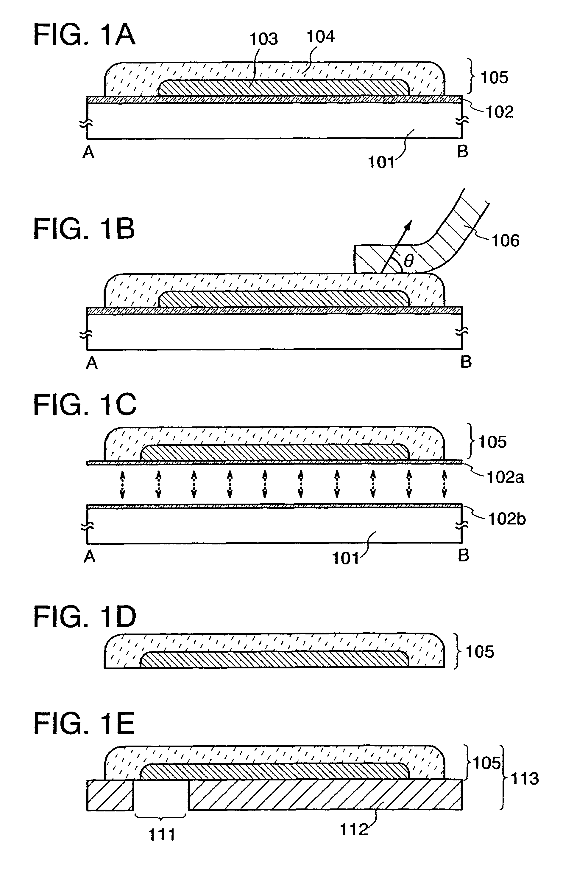
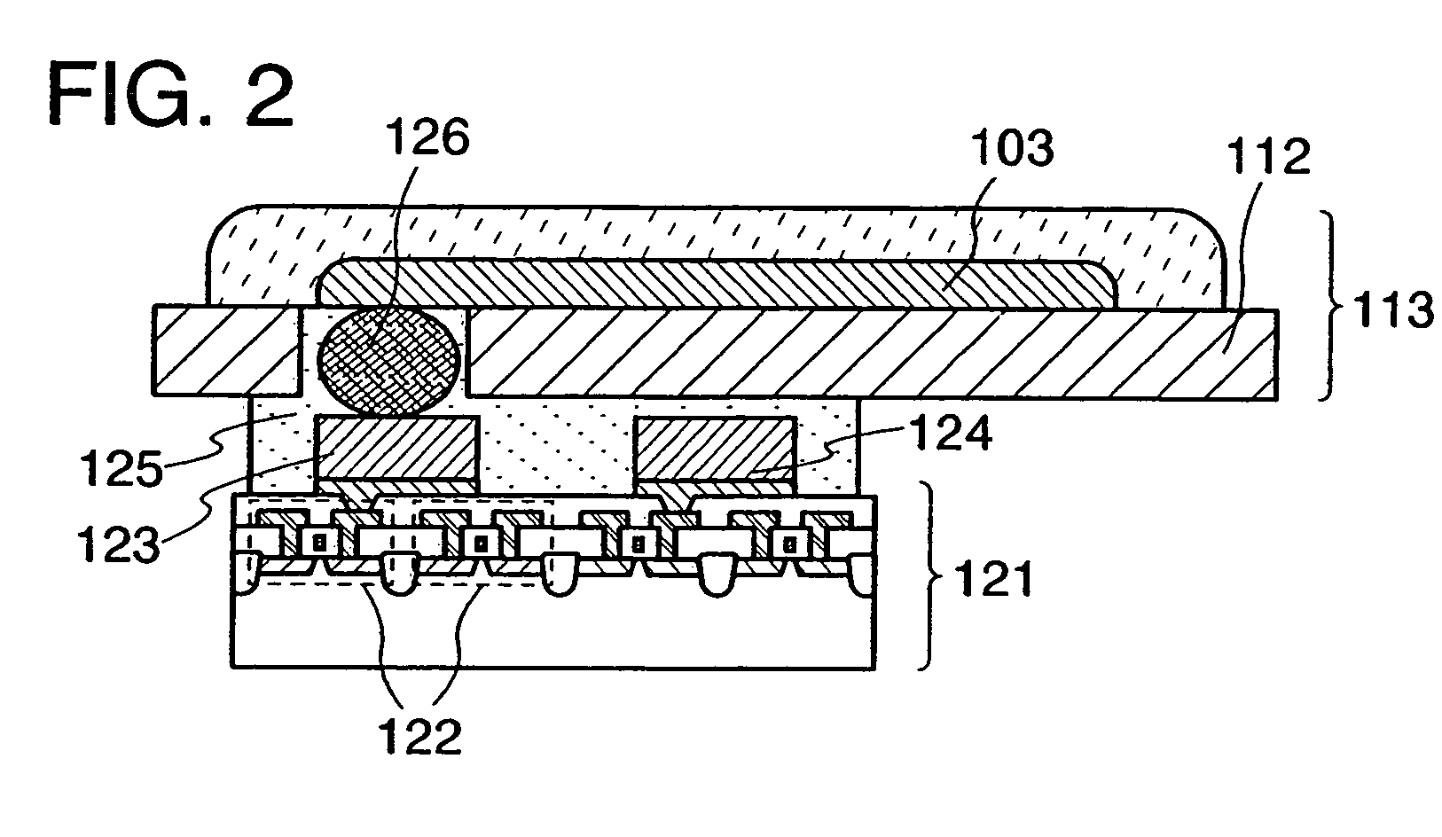
[0044]In this embodiment mode, one mode of a method for easily forming a layer having functionality will be explained with reference to FIGS. 1A to 1E, FIG. 2, FIG. 7, and FIGS. 15A and 15B. FIGS. 1A to 1E show cross-sectional views of a forming step of a layer having functionality. FIG. 2 shows a cross-sectional view of a semiconductor device capable of transmitting and receiving data wirelessly (also referred to as an RFID (Radio Frequency Identification) tag, an IC chip, an IC tag, an ID chip, an ID tag, an RF chip, an RF tag, a wireless chip, and a wireless tag). FIG. 7 shows a top view of FIG. 1A. A cross section A-B in FIG. 1A corresponds to a region A-B in FIG. 7. A layer having a conductive layer is used as a layer having functionality to explain this embodiment mode. In addition, the conductive layer here serves as an antenna. It is to be noted that this embodiment mode can be applied to a method for forming a layer having a colored layer as a layer having functionality ins...

embodiment mode 2

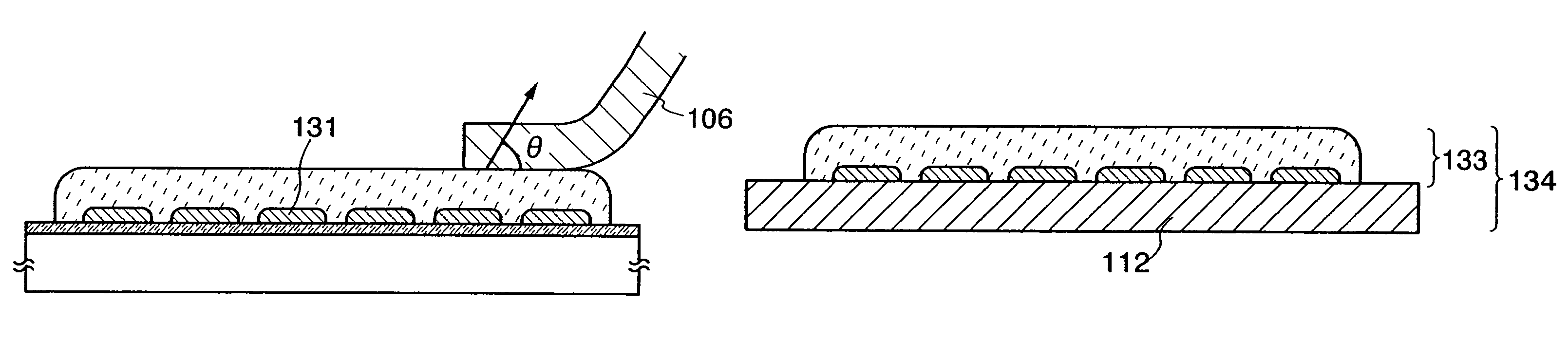
[0088]In this embodiment mode, one mode of a method for easily forming a layer having functionality will be explained with reference to FIGS. 3A to 3E and FIG 4. FIGS. 3A to 3E each show a cross-sectional view of a step for forming a layer having functionality. FIG. 4 shows a cross-sectional view of a liquid crystal display device as a display device in a case where the display device is used as a semiconductor device. A layer having a conductive layer serving as a pixel electrode is used as a layer having functionality to explain this embodiment mode.

[0089]As shown in FIG. 3A, a layer 102 in which oxygen and silicon are combined and an inactive group is combined with the silicon is formed over a substrate 101, a conductive layer 131 is formed thereover, and an insulating layer 132 covering the conductive layer 131 is formed. A functional layer 133 can be formed by the conductive layer 131 and the insulating layer 132.

[0090]The substrate 101 and the layer 102 in which oxygen and sil...

embodiment mode 3

[0100]In this embodiment mode, one mode of a method for easily forming a layer having functionality will be explained with reference to FIGS. 5A to 5E and FIGS. 6A to 6E. FIGS. 5A to 5E each show a cross-sectional view of a forming step of a layer having functionality. As a layer having functionality, a layer that optically functions such as a colored layer, a color conversion filter, or a photogram color filter can be given in this embodiment mode. Here, a colored layer is used as a layer that optically functions to explain this embodiment mode.

[0101]As shown in FIG. 5A, a layer 102 in which oxygen and silicon are combined and an inactive group is combined with the silicon is formed over a substrate 101, a colored layer is formed thereover, and an insulating layer 158 covering a colored layer is formed. Here, light shielding layers 151 to 154, a red colored layer 155, a blue colored layer 156, and a green colored layer 157 are shown as the colored layer. A functional layer 159 can ...


PUM

PropertyMeasurementUnit
temperatureaaaaaaaaaa

Abstract

It is an object of the present invention to provide a method for forming a layer having functionality including a conductive layer and a colored layer and a flexible substrate having a layer having functionality with a high yield. Further, it is an object of the present invention to provide a method for manufacturing a semiconductor device that is small-sized, thin, and lightweight. After coating a substrate having heat resistance with a silane coupling agent, a layer having functionality is formed. Then, after attaching an adhesive to the layer having functionality, the layer having functionality is peeled from the substrate. Further, after coating a substrate having heat resistance with a silane coupling agent, a layer having functionality is formed. Then, an adhesive is attached to the layer having functionality. Thereafter, the layer having functionality is peeled from the substrate, and a flexible substrate is attached to the layer having functionality.

Description

TECHNICAL FIELD[0001]The present invention relates to a layer having functionality and a method for forming a flexible substrate having the same. Further, the present invention also relates to a method for manufacturing a semiconductor device having a layer having functionality.BACKGROUND ART[0002]As a conventional method for forming a conductive layer serving as an antenna, a pixel electrode, a wiring, or the like over a flexible substrate, the following methods are given: a method in which, after a composition that contains particles with a metal element is printed over a flexible substrate by a screen printing method, the composition is heated and baked to form a conductive layer; and a method in which a conductive layer is formed over a flexible substrate by a plating method.[0003]Patent Document 1: Japanese Published Patent Application No. 2004-310502DISCLOSURE OF INVENTION[0004]In order to form a low-resistance conductive layer by using a composition that contains particles wi...

Claims


Application Information

Patent Timeline
Patent Type & Authority Patents(United States)
IPC IPC(8): H01L21/46H01L21/205H01L21/469H01L21/84H01L21/31H01L21/331H01L21/336
CPCH01Q1/38H01Q7/00H05K3/207G02F1/133305G02F1/1362H01L24/97H01L2924/01042H01L2924/01046H01L2924/01047H01L2924/01049H01L2924/01051H01L2924/01056H01L2924/01057H01L2924/01058H01L2924/0106H01L2924/01073H01L2924/01074H01L2924/01077H01L2924/01078H01L2924/01079H01L2924/01082H01L2924/09701H01L2924/10329H01L2924/14H01L2924/19041H01L2924/19043H01L2924/30107H01L2924/3025H05K3/28H05K2203/016H05K2203/0531G02F2001/13613H01L2224/16225H01L2224/97H01L2924/01002H01L2924/01004H01L2924/0101H01L2924/01013H01L2924/01015H01L2924/01018H01L2924/01027H01L2924/01029H01L2924/0103H01L2924/01032H01L2924/01033H01L2924/0104H01L2924/01005H01L2924/01006H01L2924/01023H01L2924/01024H01L2924/01041H01L2924/01044H01L2924/01045H01L2924/01067H01L2924/01068H01L2924/01072H01L2924/01076H01L2924/014H01L2924/12041H01L2924/10253H01L2924/07811H01L2924/13091H01L2224/81H01L2924/00H01L2924/15787H01L2924/15788H01L2924/12044G02F1/13613
Inventor AOKI, TOMOYUKITSURUME, TAKUYA
Owner SEMICON ENERGY LAB CO LTD
Why Eureka
Try Eureka