High resolution silicon-containing resist

a silicon-containing, high-resolution technology, applied in the field of microelectronics, can solve the problems of insufficient resist sensitivity to afford high-throughput manufacturing, reduce the integrity of the pattern, and not extendable to duv and vuv wavelengths, etc., to achieve reasonable sensitivity to imaging radiation, improve resist composition, and reduce the effect of blur

Inactive Publication Date: 2010-02-09
IBM CORP
View PDF16 Cites 2 Cited by
  • Summary
  • Abstract
  • Description
  • Claims
  • Application Information

AI Technical Summary

Benefits of technology

[0010]The invention provides improved resist compositions which are especially useful for sub-50 nm lithography, more especially where the imaging radiation is e-beam radiation. The compositions of the invention provide a combination of etch resistance toward oxygen plasma, substantially blur-free resolution, reasonable sensitivity to imaging radiation, and minimal vulnerability to airborne base contamination. The resist compositions of the invention are preferably not chemically-amplified.

Problems solved by technology

These materials offered high performance but were not extendible to DUV and VUV wavelengths due to their opacity at these shorter wavelengths.
In addition, these resists were not of sufficient sensitivity to afford high throughput manufacturing.
One barrier to imaging in the sub-50 nm half-pitch regime is a phenomenon known as image blur which diminishes the integrity of the pattern.
While accelerating the rate of the deprotection reaction, the application of thermal energy diminishes the fidelity of the aerial image of acid formed during the patternwise exposure.
However, these approaches only reduce the image blur to low blur imaging.
At such scale, blur is especially problematic.
Conventional DNQ systems are non-CA resists which have poor performance in E-beam lithography.
Side chain scission with a minute quantum yield of 10−6 has also been reported, but is too inefficient for practical resist applications.
Another well known non-CA E-beam resists are based on polybutene sulfone, however, these resists are not etch resistant (for reactive ion etching (RIE)), and thus the pattern cannot be transferred by a RIE process.
Multilayer resist systems are generally more complex and expensive to implement.

Method used


Image

  • High resolution silicon-containing resist
  • High resolution silicon-containing resist
  • High resolution silicon-containing resist

Examples


example 1

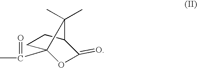
Synthesis of Camphanic Group Partially Protected Poly(2-Hydroxy-3,3,3-Trifluoropropylsilsesquioxane) (FSQ-CAF)

[0060]7 g of poly(2-hydroxy-3,3,3-trifluoropropylsilsesquioxane) (FSQ) and 4.14 g of camphanic chloride were dissolved in 35 g of GBL and charged into a 100 ml flask. The mixture was stirred under ice bath, while 1.93 g of 4-methylmorpholine was added into the mixture dropwise within 20 minutes. After approximately two hours stirring under the ice bath temperature, the reaction mixture was allowed to warm up slowly to the room temperature and the reaction was continued overnight. The solution was then precipitated in 2000 ml DI water. The resulting gel-like polymer was redissolved in acetone and reprecipitated in 2000 ml DI water. The polymer was collected and dried in vacuum oven overnight at 65° C.

example 2

Dissolution Rate and Optical Property Measurements of FSQ-CAF

[0061]800 mg of FSQ-CAF synthesized in Example 1 above was dissolved in PGMEA to a total weight of 10 g providing the solid content of the polymer in the solution is 8%. This radiation sensitive resist composition was then spin-coated on quartz disk and baked at 110° C. for 60 s. The disk containing resist film was then developed in 0.263N TMAH developer and monitored with Research Quartz Crystal Microbalance (RQCM, RS-232) tool manufactured by Maxtek, Inc. The dissolution rate of FSQ-CAF in comparison to that of FSQ is shown in Table 1 below.

[0062]

TABLE 1Dissolution rates evaluationPolymerDissolution rateFSQ 11.3 nm / sFSQ-CAF0.134 nm / s

[0063]To measure the optical properties, the resist composition above was spin coated onto silicon wafers, baked on hot plate at 110° C. for 60 s, and then n and k values were measured with VB-250 VASE Ellipsometer manufactured by J.A. Woollam Co. Inc. The optical properties of the resist com...

example 3

E-beam Imaging Evaluation

[0065]Resist formulation with 8% FSQ-CAF in Example 2 was spin coated with 2500 rpm on HMDS primed wafers. The resist was baked on a hot plate at 110° C. for 1 minute to give ˜100 nm thick film. The exposures were performed on a 100 kV Leica exposure system. After exposure, the resist was developed with 0.263N TMAH for 60 s. High resolution of 60 nm l / s images was obtained at 420 μC / cm2 with resist lines standing, and 50 nm l / s images were resolved with some lines collapsed. The contrast of the resist is around 3.


PUM

PropertyMeasurementUnit
wavelengthsaaaaaaaaaa

Abstract

Non-chemically amplified radiation sensitive resist compositions containing silicon are especially useful for lithographic applications, especially E-beam lithography. More particularly, radiation-sensitive resist compositions comprising a polymer having at least one silicon-containing moiety and at least one radiation-sensitive moiety cleavable upon radiation exposure to form aqueous base soluble moiety can be used to pattern sub-50 nm features with little or no blur.

Description

STATEMENT OF GOVERNMENT INTEREST[0001]This invention was made with Government support under Contract No. N-66001-00-C-8083 awarded by the Department of the Navy, Space and Warfare Systems Center. The Government has certain rights in this invention.BACKGROUND OF THE INVENTION[0002]In the microelectronics industry, there is a continued desire to reduce the size of structural features and / or to provide greater amount of circuitry for a given chip size. Advanced lithographic techniques are required to fabricate high performance and high density circuitry. Lithography impacts the manufacture of microscopic structures not only in terms of directly imaging patterns on the desired substrate, but also in terms of making masks typically used in such imaging.[0003]Over approximately the last 20 years, the industry has migrated to shorter wavelength photolithography as the primary means of scaling the resolution to sustain the progressive demand for smaller features. The wavelength of imaging r...

Claims


Application Information

Patent Timeline
Patent Type & Authority Patents(United States)
IPC IPC(8): H01L21/00G03C1/00
CPCG03F7/0045G03F7/0757G03F7/0046
Inventor BUCCHIGNANO, JAMES J.HUANG, WU-SONG S.KLAUS, DAVID P.SEKARIC, LIDIJAVISWANATHAN, RAMAN G.
Owner IBM CORP
Why Eureka
Try Eureka