Semiconductor device including a current mirror circuit

a technology of mirror circuit and semiconductor element, which is applied in the direction of electric variable regulation, process and machine control, instruments, etc., can solve the problems of destabilization of operation, deformation of output current value, and deterioration of parasitic resistance in each of the tfts that form the amplifier circuit. achieve the effect of high-precision produ

Inactive Publication Date: 2010-02-23
SEMICON ENERGY LAB CO LTD
View PDF20 Cites 20 Cited by
  • Summary
  • Abstract
  • Description
  • Claims
  • Application Information

AI Technical Summary

Benefits of technology

[0006]Most of the conventional amplifier circuits have a multistage configuration including a correction circuit, which needs high power supply voltage. At present, it has been necessary to stably supply power supply voltage in forming an electric circuit in terms of energy saving, high performance, and the like.
[0015]In the present invention, the thin film transistors each have an island-shaped semiconductor film having a channel formation region and source or drain regions, a gate insulating film, a gate electrode, and source or drain electrodes, and the compensation resistor compensates parasitic resistance of the gate electrode.
[0016]In the present invention, the thin film transistors each have an island-shaped semiconductor film having a channel formation region and source or drain regions, a gate insulating film, a gate electrode, and source or drain electrodes, and the compensation resistor compensates parasitic resistance of the source electrode.
[0017]In the present invention, the thin film transistors each have an island-shaped semiconductor film having a channel formation region and source or drain regions, a gate insulating film, a gate electrode, and source or drain electrodes, and the compensation resistor compensates parasitic resistance of the drain electrode.
[0023]A semiconductor device of the present invention has a function to operate an amplifier circuit stably by compensation of various parasitic resistance due to a resistor being added. Due to the stable amplifier circuit, the operating voltage of a bias circuit can be uniformed and the electric characteristics of the circuit can be uniformed; thus, a more highly precise product can be supplied.

Problems solved by technology

However, the amplifier circuit including TFTs as described above has a problem that the operation is destabilized by parasitic resistance due to wiring resistance, contact resistance, or the like of conductive layers that form the TFTs or wirings connected to the conductive layers.
It can be considered that the cause of destabilization in operation of the amplifier circuit is that conductive layers that form the TFTs or wirings connected to the conductive layers are formed of different materials, or, since the width or length thereof are different, the value of the parasitic resistance is different; thus, the balance of the parasitic resistance in each of the TFTs that form the amplifier circuit is deteriorated.
Due to the destabilization in operation of the amplifier circuit, an output current value thereof is destabilized.

Method used


Image

  • Semiconductor device including a current mirror circuit
  • Semiconductor device including a current mirror circuit
  • Semiconductor device including a current mirror circuit

Examples


embodiment 1

[0191]A case of applying this embodiment to a semiconductor device including a photoelectric conversion device will be explained with reference to FIGS. 15, 16, FIGS. 17A to 17C, FIGS. 18A to 18C, FIGS. 19A and 19B, FIGS. 20A to 20C, and FIG. 32. Note that the same portions as explained in embodiment mode are denoted by the same reference numerals.

[0192]First, an element is formed over a substrate (a first substrate 210). Here, AN 100 which is one of glass substrates is used for the substrate 210.

[0193]Next, a silicon oxide film containing nitrogen (100 nm thick) to be a base insulating film 212 is formed by a plasma CVD method, and further, without being exposed to the atmosphere, a semiconductor film, for example, an amorphous silicon film containing hydrogen (54 nm thick) is formed to be stacked. In addition, the base insulating film 212 may also be formed using the stack of a silicon oxide film, a silicon nitride film, and a silicon oxide film containing nitrogen. For example, a...

embodiment 2

[0254]This embodiment will explain an example of forming an amplifier circuit with a p-channel TFT with reference to FIG. 5 and FIG. 26. Note that the same portions as in Embodiment Mode and Embodiment 1 are denoted by the same reference numerals, and the same portions may be formed based on the manufacturing process described in Embodiment Mode and Embodiment 1.

[0255]This embodiment will show an example of applying the resistors shown in FIG. 11 to resistors for compensating parasitic resistors. However, this embodiment is not limited thereto and the resistors shown in FIGS. 6 to 10 may also be applied.

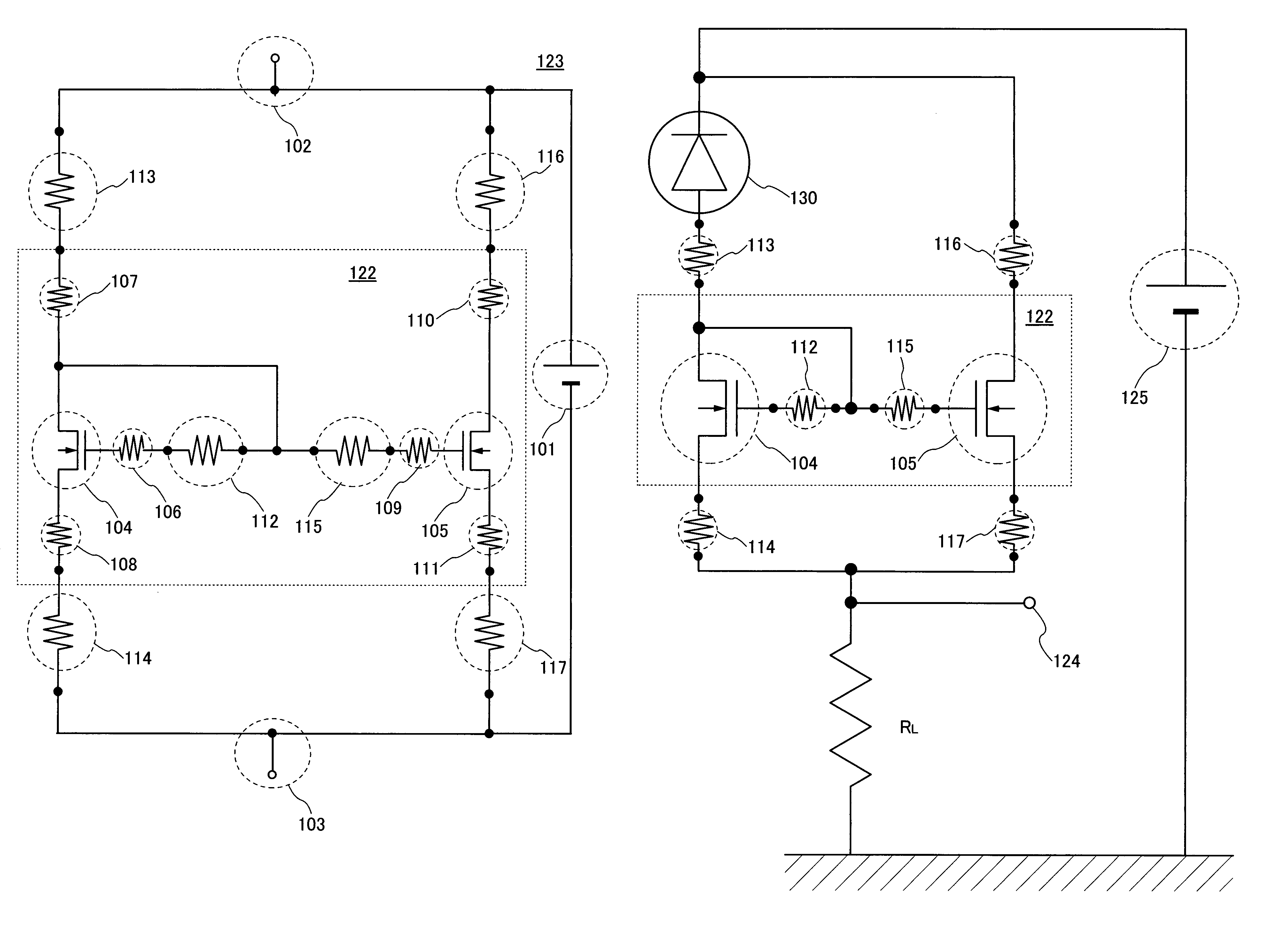
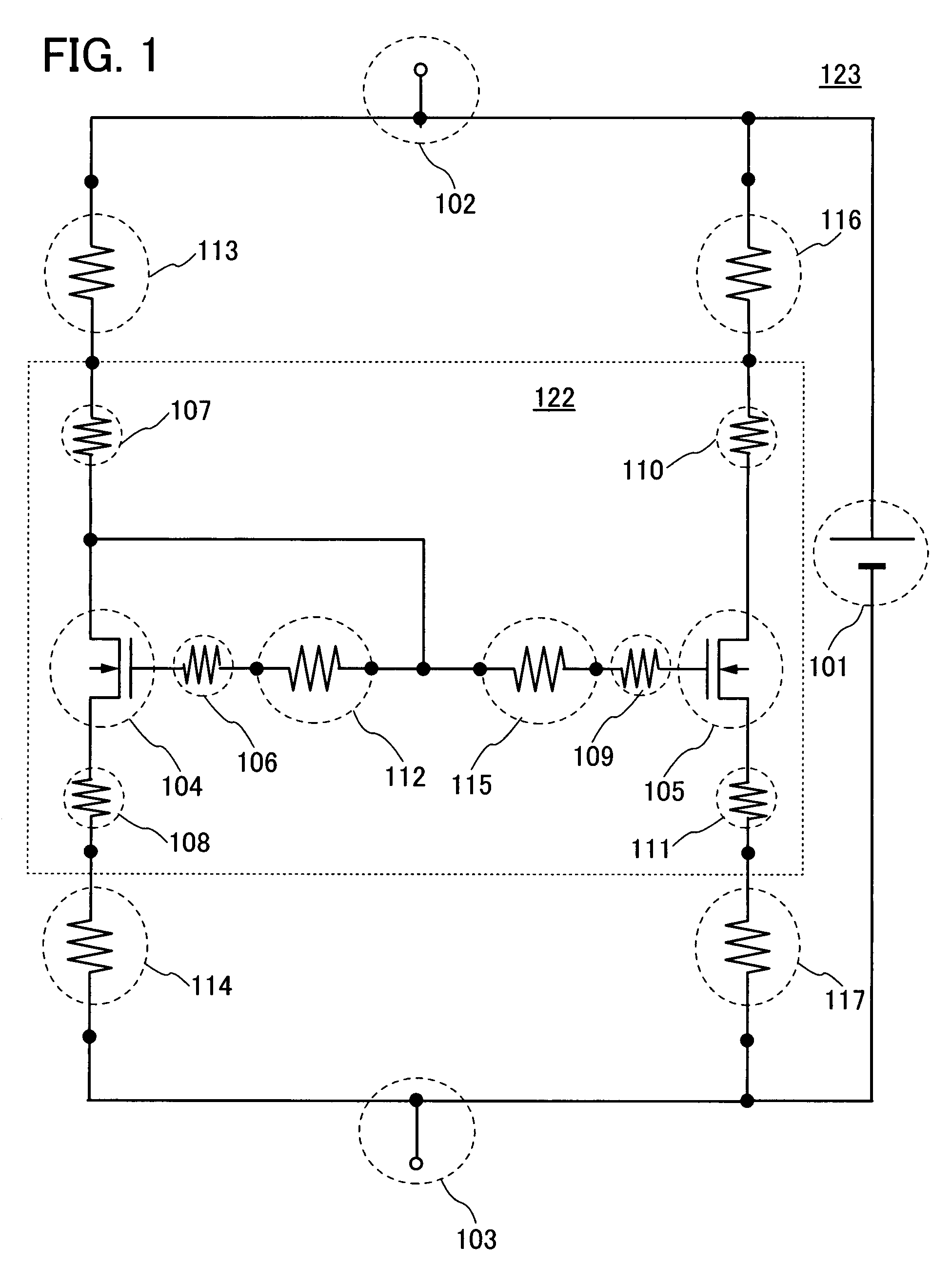
[0256]In a case where an amplifier circuit, for example, a current mirror circuit 203 is formed of p-channel TFTs 201 and 202, a p-type impurity, for example, boron (B) may be substituted for the impurity imparting one conductivity type to the island-shaped semiconductor region in Embodiment Mode and Embodiment 1.

[0257]FIG. 5 shows an equivalent circuit diagram of a light sensor of t...

embodiment 3

[0265]This embodiment will explain an example of a light sensor in which an amplifier circuit is formed using a bottom gate TFT and a manufacturing method thereof with reference to FIGS. 27A to 27D, FIGS. 28A to 28C, FIGS. 29A and 29B, FIG. 30, FIG. 31, FIG. 38, FIG. 39, FIG. 40, FIG. 41, and FIG. 42. Note that the same portions as in Embodiment Mode and Embodiments 1 and 2 are denoted by the same reference numerals.

[0266]First, a base insulating film 212 and a metal film 311 are formed over a substrate 210 (see FIG. 27A). As the metal film 311, in this embodiment, a film in which tantalum nitride (TaN) of 30 nm thick and tungsten (W) of 370 nm thick are stacked is used, for example.

[0267]In addition, as the metal film 311, as well as the above film, a single-layer film formed of an element of tungsten (W), tantalum (Ta), molybdenum (Mo), neodymium (Nd), cobalt (Co), zirconium (Zr), zinc (Zn), ruthenium (Ru), rhodium (Rh), palladium (Pd), osmium (Os), iridium (Ir), platinum (Pt), al...


PUM


Abstract

In a semiconductor device, where, with respect to a parasitic resistor in a current mirror circuit, a compensation resistor for compensating the parasitic resistor is provided in the current mirror circuit, the current mirror circuit includes at least two thin film transistors. The thin film transistors each have an island-shaped semiconductor film having a channel formation region and source or drain regions, a gate insulating film, a gate electrode, and source or drain electrodes, and the compensation resistor compensates the parasitic resistor of any one of the gate electrode, the source electrode, and the drain electrode. In addition, each compensation resistor has a conductive layer containing the same material as the gate electrode, the source or drain electrodes, or the source or drain regions.

Description

BACKGROUND OF THE INVENTION[0001]1. Field of the Invention[0002]The present invention relates to a semiconductor device, particularly a semiconductor device including a thin film semiconductor element, and a manufacturing method thereof.[0003]2. Description of the Related Art[0004]In general, a current mirror circuit is used in many cases as part of a power supply circuit of a display or the like. The power supply circuit includes an analog circuit, and the performance of a bias circuit is important as the stable operation. It is important to design a bias circuit in a case of designing a high-performance analog circuit or a low-voltage operation circuit.[0005]In conventional amplifier circuits, there are some of them, the performance of which is improved by multistage connection of thin film transistors (TFTs) (for example, see Patent Document 1: Japanese Published Patent Application No. H6-37558).SUMMARY OF THE INVENTION[0006]Most of the conventional amplifier circuits have a mult...

Claims


Application Information

Patent Timeline
Patent Type & Authority Patents(United States)
IPC IPC(8): H01L23/62
CPCG05F3/262H01L21/84H03F1/086H01L27/12H03F2200/513H01L2224/16225
Inventor HIROSE, ATSUSHI
Owner SEMICON ENERGY LAB CO LTD
Why Eureka
Try Eureka