Electromagnetic wave absorber

a technology of electromagnetic waves and absorbers, applied in waveguides, screening rooms/chambers, and antennas, etc., can solve the problems of lowering the transmission speed between equipment using wireless technologies, deteriorating ber (bit error rate), and affecting the absorption efficiency of electromagnetic waves

Inactive Publication Date: 2010-09-28
NITTA CORP
View PDF41 Cites 26 Cited by
  • Summary
  • Abstract
  • Description
  • Claims
  • Application Information

AI Technical Summary

Benefits of technology

[0013]It is an object of at least one embodiment of the invention to provide an electromagnetic wave absorber that is thin, light, soft, and excellent in the strength and workability while having a high ability to absorb electromagnetic waves.

Problems solved by technology

In an environment in which a large number of such technologies are used together with one another, there are problems in that electromagnetic waves interfere with each other when electromagnetic waves in the same band are used or in that transmission errors (multi-path) are caused by reflected waves and the like.
More specifically, the transmission speed between equipment using the wireless technologies is lowered, and BER (bit error rate) is deteriorated, and in the worst case, the equipment may malfunction.
In this conventional technique, for example, when an electromagnetic wave absorber is realized using ferrite as a constituent in the 2.45 GHz band of a wireless LAN and the like, there is a problem in that due to the restriction of the snoek peak, it is usually impossible to reduce the thickness of the electromagnetic wave absorbing material to 4 mm or less.
Since the absorption frequency is controlled only with the shape of patterns and the interval of spacers, when the thickness of the spacers is changed by the incident angle of radio waves, the oblique incident property becomes poor.
However, this method involves various factors to be calculated, and when actually combined with a material used as an architectural interior material with a different complex relative dielectric constant, for example, it is complicated to change the design.
It is difficult to make an absorber thin and to sustain a high strength thereof while keeping a high absorbing ability.
In particular, for an electromagnetic wave absorber for absorbing radio waves with a lower frequency such as 1 to 3 GHz, it is necessary that the absorber layer is thick, and thus it is difficult to make the absorber thinner and lighter, and to attain softness and processability in being cut on the spot.
In particular, when a wireless LAN is actually used, metal racks, posts, or air conditioners that have been conventionally present act as electromagnetic wave reflecting layers, and thus there are spots with poor wireless communications.
In this case, covering a portion exerting an influence on the wireless communication environment with an electromagnetic wave absorbing member is effective in improving communications, but conventional techniques cannot provide a radio wave absorber that is thin, light, soft, and excellent in the strength and workability while having a high ability to absorb radio waves.
A loss material is provided close to the element receiving means, and causes energy loss to electromagnetic waves that are received by the element receiving means.
In this case, when the shape of the pattern is simple, modeling as an equivalent circuit is easy, but when the shape is complicated, it is theoretically difficult to form an equivalent circuit, and thus it is difficult to optimize the shape of the pattern.
The reason for this is that in particular, when a conductive reflecting layer is provided close thereto, a capacitor with a large capacity is formed between the conductor elements and the conductive reflecting layer, and this capacitor exerts an influence on the resonant frequency, and it is very difficult to eliminate this influence.
More specifically, the resonant frequency of the receiving elements is changed at each arrangement location, and thus the electromagnetic wave absorber cannot be used as an electromagnetic wave absorber corresponding to the frequency that was assumed at the time of designing.
As the conductor elements, various materials such as metal and conductive ink can be used, but there is a limitation regarding the conductivity.
It is impossible to stably attain a conductivity of at least 10,000 S / m described above in conductive ink made of carbon or black lead.
When the thickness is more than 4 mm, there is a problem in making the absorber thinner and lighter, and the flexibility is lowered.
When the mass is more than 5 kg / m2, there is a problem in making the absorber thinner and lighter, and the thickness is increased and the flexibility is lowered.

Method used


Image

  • Electromagnetic wave absorber
  • Electromagnetic wave absorber
  • Electromagnetic wave absorber

Examples


example 1

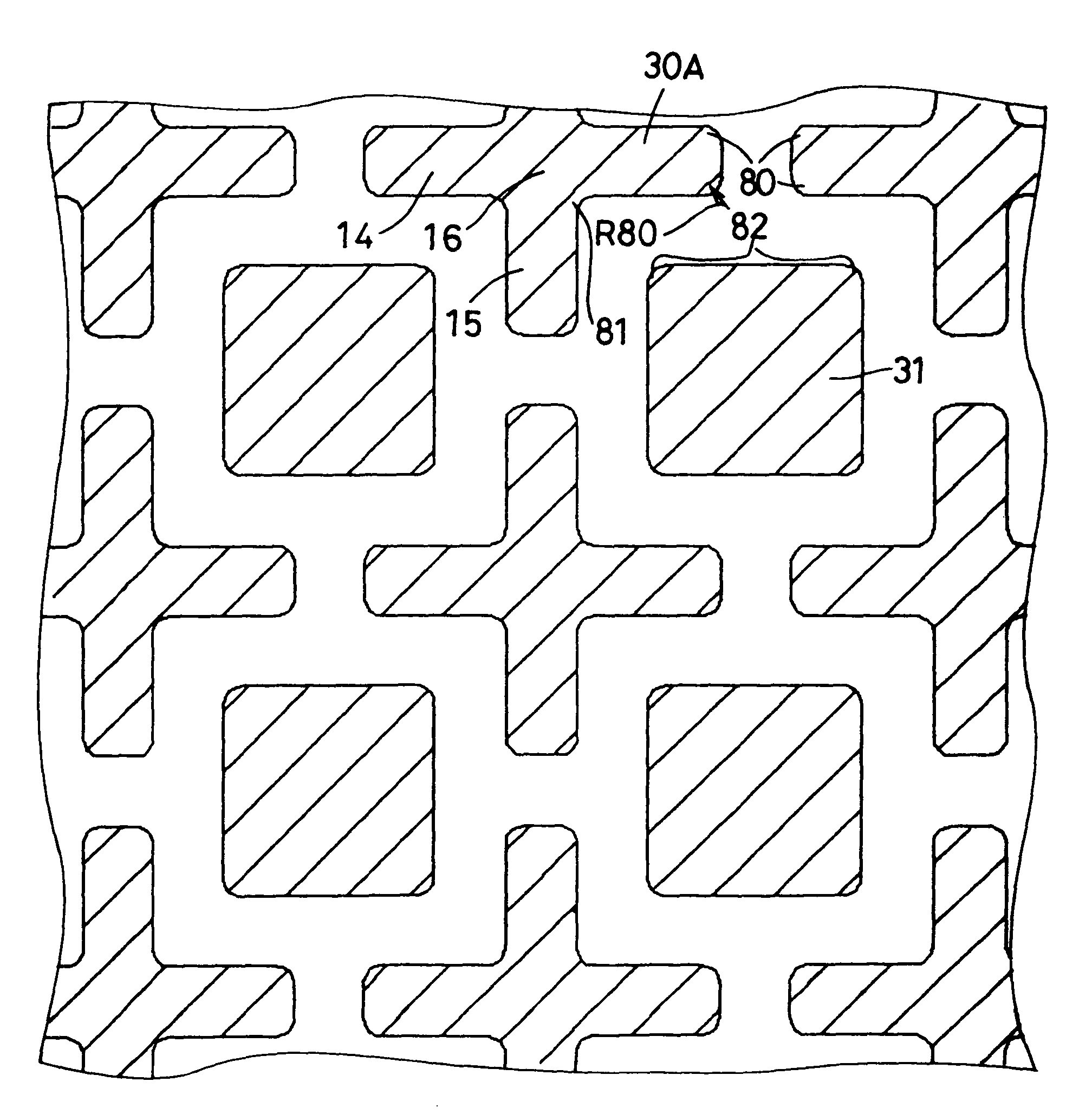
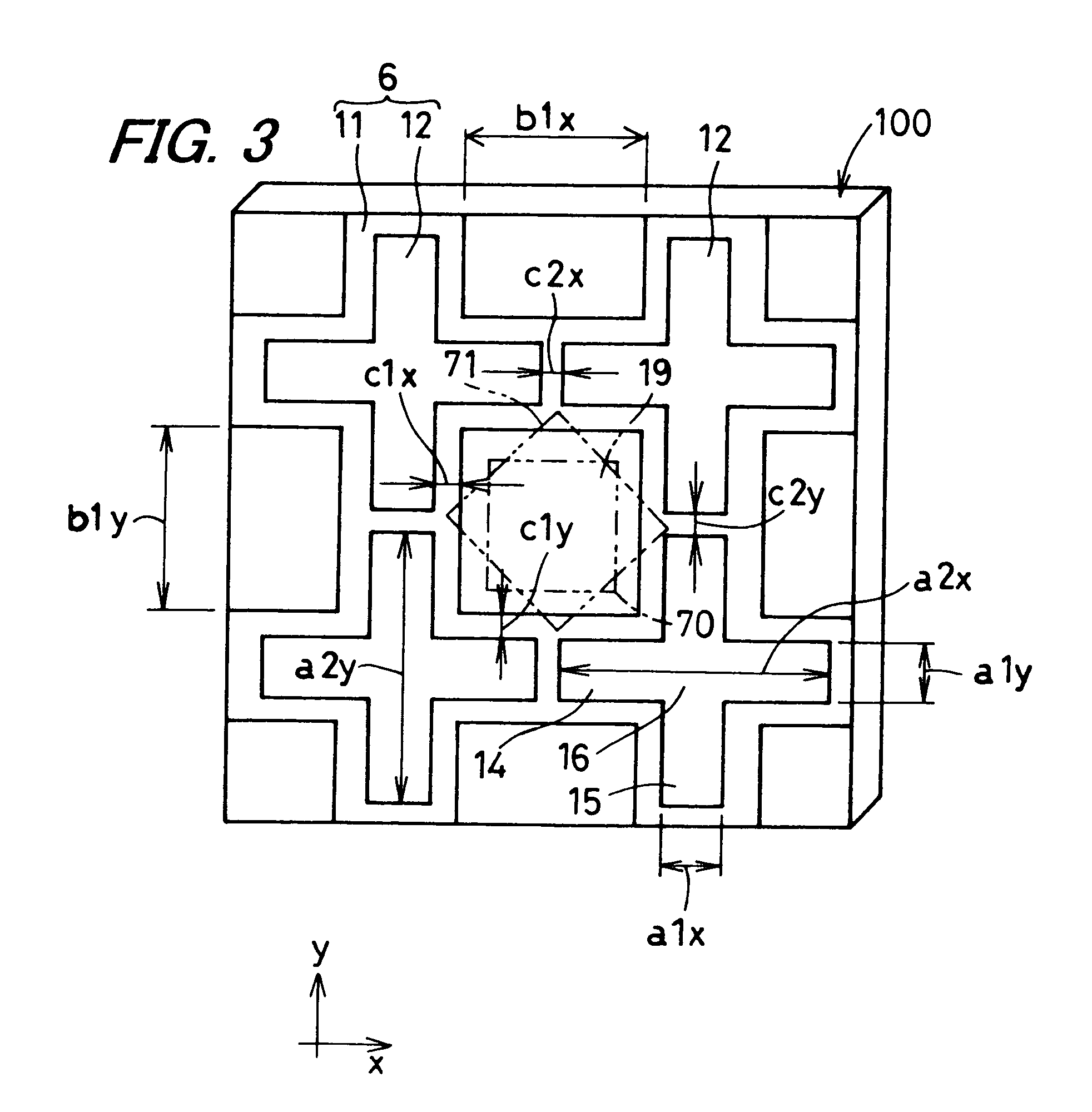
[0130]The electromagnetic wave reflecting plate 2 is an aluminum-evaporated polyethylene terephthalate (PET) film, for example. As the second loss material layer 3, a polyethylene resin foam is used, in which the complex relative dielectric constant (real part) ∈ is 1.25 (2.4 GHz) and the thickness is 1.5 mm. As the first loss material layer 5, 100 parts by weight of chloroprene rubber, 8 parts by weight of Ketjenblack EC (product name, produced by LION AKZO CO., LTD.) as a dielectric loss material, and 100 parts by weight of powder of ferrite (product name: KNS-415, produced by TODA KOGYO CORP.) as a magnetic loss material are kneaded, and then vulcanized and molded into a sheet (thickness: 1 mm).

[0131]At that time, the complex relative dielectric constant and the complex relative permeability of the vulcanized rubber sheet were measured by a coaxial cylinder method (S-parameter method). Considering the results thereof and lamination conditions of the electromagnetic wave absorber ...

example 2

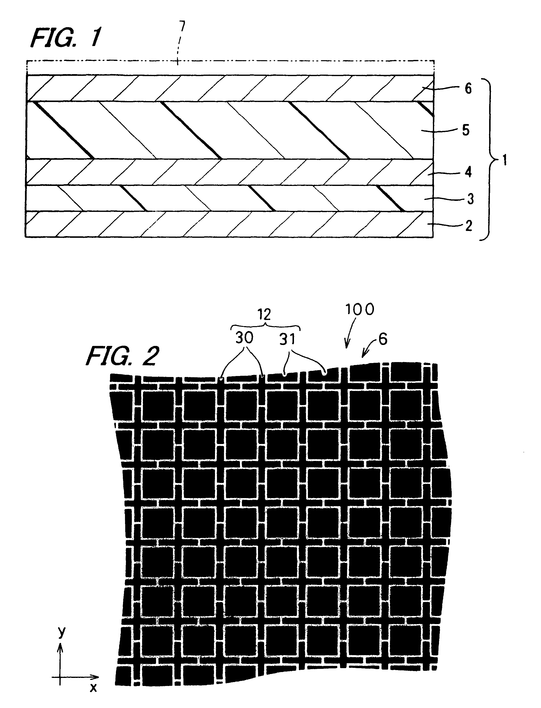
[0140]In the configuration of Example 2, the first conductor element layer 6 in which the shape of conductor elements is the same as that in Example 1 is used, and the second conductor element layer 4 is not used. FIG. 17 is a graph showing the results obtained with the configuration without the second conductor element layer 4. The first loss material layer 5 is constituted by two layers, including the layer closer to the first conductor element layer 6 that is 0.5 mm of PVC (vinyl chloride resin) to which ferrite and carbon black have been added, and 2 mm of PET to which ferrite has not been added, and the electromagnetic wave absorber 1 with a total thickness of 2.5 mm is thus configured. In the PVC layer, the dielectric constant is 16 in the real part and 3 in the imaginary part (2.4 GHz), and the permeability is 1.43 in the real part and 0.5 in the imaginary part (2.4 GHz). In the PET, the dielectric constant is 3.1 (2.4 GHz), and the permeability is 1 in the real part and 0 in...

example 3

[0143]In the configuration of Example 3, the first conductor element layer 6 in which the shape of conductor elements is the same as that in Example 1 is used, and the second conductor element layer 4 is not used. FIG. 18 is a graph showing the results obtained with the configuration without the second conductor element layer 4. The first loss material layer 5 is constituted by two layers, including the layer closer to the first conductor element layer 6 that is 0.5 mm of PVC (vinyl chloride resin) to which ferrite and carbon black have been added, and 1 mm of PVC to which ferrite has not been added, and the electromagnetic wave absorber 1 with a total thickness of 1.5 mm is thus configured. In the PVC layer, the dielectric constant is 16 in the real part and 3 in the imaginary part (2.4 GHz), and the permeability is 1 in the real part and 0 in the imaginary part (2.4 GHz). In the PET, the dielectric constant is 3.1 (2.4 GHz), and the permeability is 1 in the real part and 0 in the ...


PUM


Abstract

A thin, light and soft electromagnetic wave absorber is disclosed exhibiting an excellent workability. The first conductor element group of a first conductor element layer consists of aligned cross conductor elements and square conductor elements in regions surrounded by cross conductor elements. A radio wave incident from the first conductor element layer side is received by each element, internally subjected to multiple reflection and then absorbed by a first loss material layer. Since the first conductor element group is realized by the cross conductor elements and the square conductor elements, receiving effect is enhanced and the radio wave can be collected with a high collection efficiency.

Description

PRIORITY STATEMENT[0001]This application is the national phase under 35 U.S.C. §371 of PCT International Application No. PCT / JP2004 / 002503 which has an International filing date of Mar. 1, 2004, which designated the United States of America, the entire contents of which are hereby incorporated herein by reference.TECHNICAL FIELD[0002]The present invention generally relates to an electromagnetic wave absorber used for improving an electromagnetic environment in space such as offices.BACKGROUND ART[0003]Currently, in the architecture of LANs (local area networks) on computer networks, communication systems with better flexibility and higher mobility have been developed using, for example, wireless LANs with micro waves. Furthermore, a short-range wireless technology called Bluetooth, which is said to represent a WPAN (wireless personal area network), is used instead of wired cables. In an environment in which a large number of such technologies are used together with one another, ther...

Claims


Application Information

Patent Timeline
Patent Type & Authority Patents(United States)
IPC IPC(8): H01Q17/00H05K9/00
CPCH01Q17/002H05K9/0003H05K9/00
Inventor YOSHIDA, TAKAHIKOGO, HARUHIDEKIYOHARA, YOSHIHARUSATO, SHINICHIMAEZAWA, MAKOTOMAENAKA, MAMORU
Owner NITTA CORP
Why Eureka
Try Eureka