Spray pyrolysis for large-scale production of chalcopyrite absorber layer in photovoltaic devices

Active Publication Date: 2010-11-23
GLOBALFOUNDRIES US INC
View PDF19 Cites 20 Cited by
  • Summary
  • Abstract
  • Description
  • Claims
  • Application Information

AI Technical Summary

Benefits of technology

[0020]In yet another aspect of the invention, a spray pyrolysis system is provided. The spray pyrolysis system includes a reservoir adapted for storing a precursor solution of metal chalcogenide dissolved in hydrazine or a hydrazine-like solvent; a nozzle adapted to receive the precursor solution from the reservoir via one or more fluid conduit

Problems solved by technology

However, due to high production costs and low light-to-energy conversion efficiencies associated with conventional photovoltaic technology, photovoltaic devices have not yet gained widespread use.
For example, traditional photovoltaic devices rely on costly high quality silicon (Si), an indirect bandgap material, and involve multi-step vacuum processes during production.
Vacuum-based deposition processes for CIGS compounds are, however, expensive.
Namely, expensive vacuum equipment, a sophisticated flux control setup and constant heating during the deposition all contribute to high production costs.
Further, material utilization is not very efficient as a s

Method used


Image

  • Spray pyrolysis for large-scale production of chalcopyrite absorber layer in photovoltaic devices
  • Spray pyrolysis for large-scale production of chalcopyrite absorber layer in photovoltaic devices
  • Spray pyrolysis for large-scale production of chalcopyrite absorber layer in photovoltaic devices

Examples


Embodiment Construction

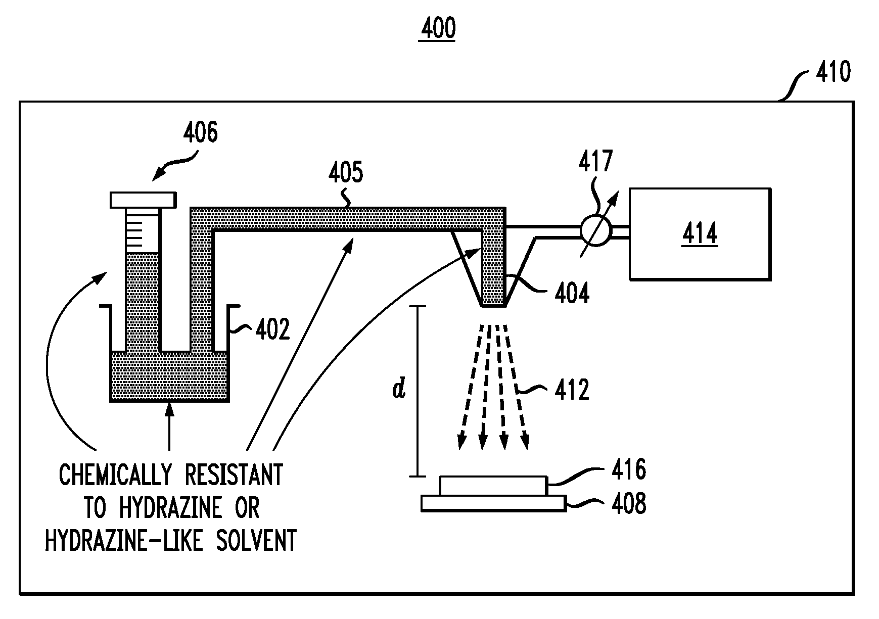
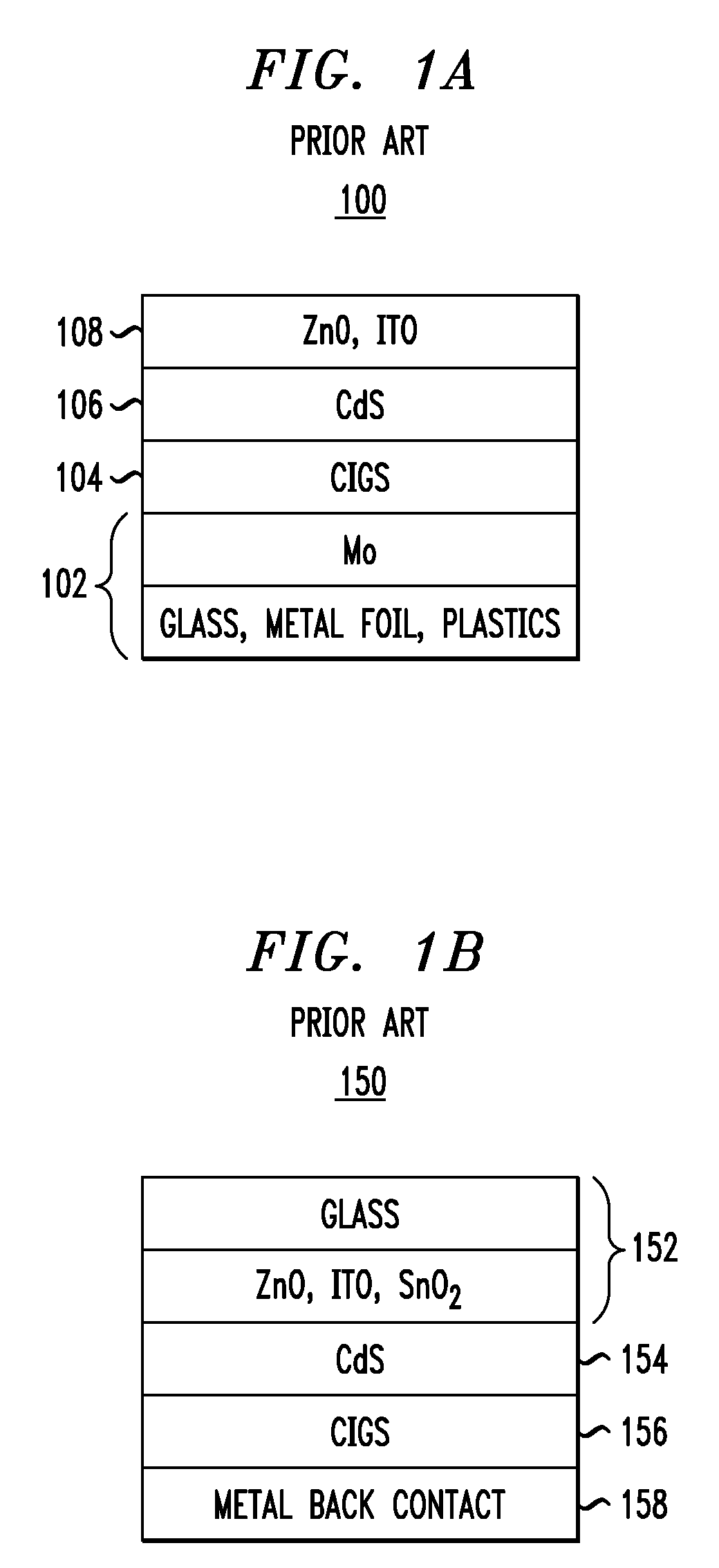
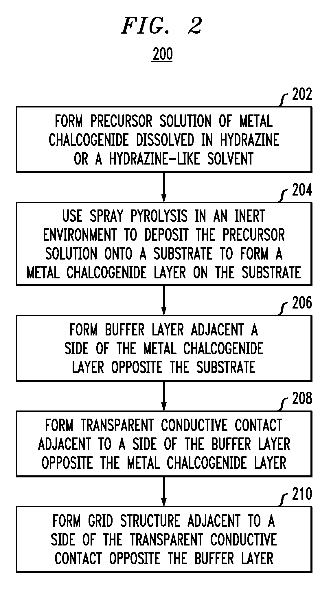
[0027]FIG. 2 is a diagram illustrating exemplary methodology 200 for fabricating a photovoltaic device with a substrate configuration. Methodology 200 provides an improved, low-cost, solution-based technique to grow uniform large-area copper indium gallium selenide / sulfide (CIGSS) absorber layers for photovoltaic applications. As will be described in detail below, the present techniques involve a spray-based deposition process, which produces substrate structure CIGSS solar cells using metal chalcogenides homogenously dissolved in hydrazine or a hydrazine-like solvent, such as ethanolamine and / or dimethyl sulfoxide (DMSO). As highlighted above, the use of a substrate structure as opposed to a superstrate structure allows for better grain growth in the CIGSS absorber layer through high temperature heat treatments without the possibility of damaging the later-formed p-n junction (i.e., between the CIGSS absorber layer and a buffer layer, see below).

[0028]In step 202, a precursor solut...


PUM

PropertyMeasurementUnit
Temperatureaaaaaaaaaa

Abstract

Techniques for fabricating a photovoltaic device having a chalcopyrite absorber layer, such as a copper indium gallium selenide/sulfide (CIGSS) absorber layer, are provided. In one aspect, a method for fabricating a photovoltaic device is provided. The method includes the following steps. A precursor solution of metal chalcogenide dissolved in hydrazine or a hydrazine-like solvent is formed. Spray pyrolysis in an inert environment is used to deposit the precursor solution onto a substrate to form a metal chalcogenide layer on the substrate. A buffer layer is formed adjacent to a side of the metal chalcogenide layer opposite the substrate. A transparent conductive contact is formed adjacent to a side of the buffer layer opposite the metal chalcogenide layer.

Description

FIELD OF THE INVENTION[0001]The present invention relates to photovoltaic devices, and more particularly, to techniques for fabricating a photovoltaic device having a chalcopyrite absorber layer such as a copper indium gallium selenide / sulfide (CIGSS) absorber layer.BACKGROUND OF THE INVENTION[0002]Skyrocketing crude oil prices coupled with a dramatic rise in worldwide energy demands and increased concerns regarding environmental pollution and global warming make clean renewable energy a necessity for future energy needs. Among all renewable energies, solar power is clean, abundant and distributed virtually everywhere around the world. Photovoltaic devices take advantage of the enormous solar energy source and directly transfer sunlight into electricity.[0003]However, due to high production costs and low light-to-energy conversion efficiencies associated with conventional photovoltaic technology, photovoltaic devices have not yet gained widespread use. For example, traditional photo...

Claims


Application Information

Patent Timeline
IPC IPC(8): H01L21/20
CPCC23C18/1204C23C18/1225C23C18/1241C23C18/1258H01L21/02568H01L21/02628H01L31/0322Y02E10/541
Inventor LIU, WEIMITZI, DAVID B.
Owner GLOBALFOUNDRIES US INC
Why Eureka
Try Eureka