

Techniques for Forming a Chalcogenide Thin Film Using Additive to a Liquid-Based Chalcogenide Precursor
a technology of chalcogenide and additives, applied in the field of photovoltaic devices, can solve the problems of poor film morphology, affecting device performance, and difficult control of grain structure and film morphology of the absorber layer, so as to improve grain structure and film morphology, and enhance energy conversion efficiency
- Summary
- Abstract
- Description
- Claims
- Application Information
AI Technical Summary
Benefits of technology
Problems solved by technology
Method used
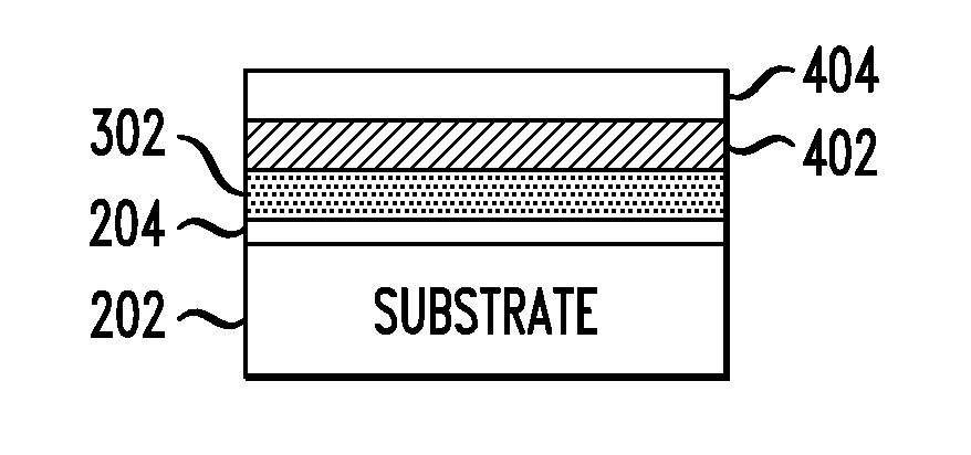
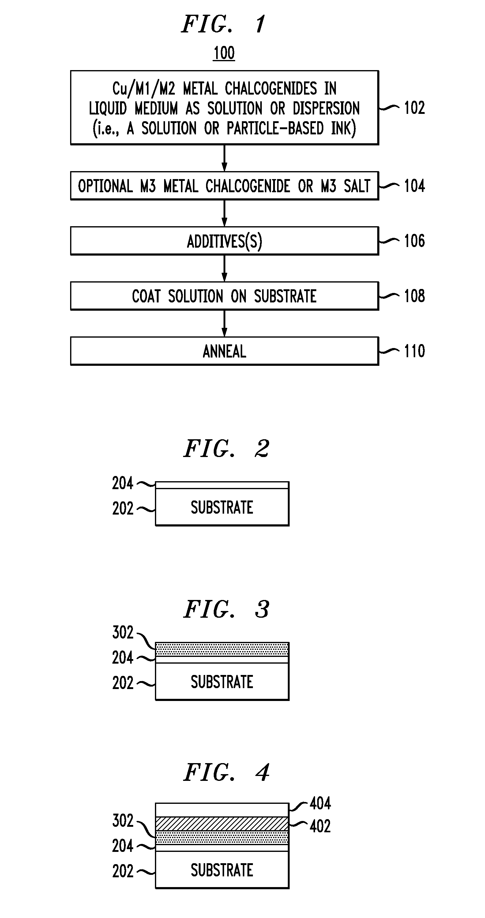
Image

Examples
example 1
CZTS Device Absorber Layer Preparation Using Urea as Additive
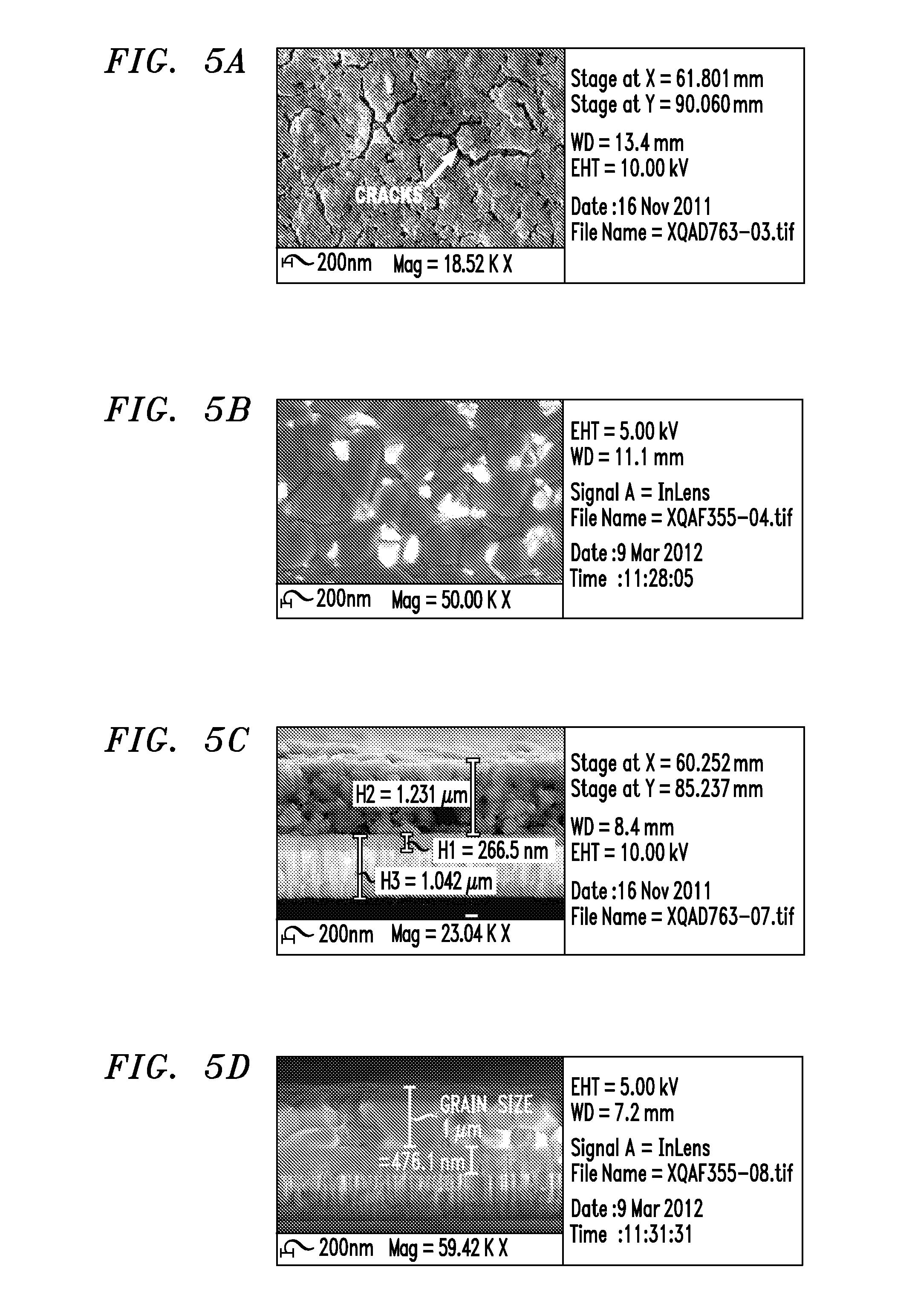
[0082]1. The preparation of precursor ink for thin film deposition: An aqueous ink was prepared by first dissolving 1.015 g of copper(II) chloride (CuCl2, 99.99%, anhydrous from Sigma-Aldrich), 0.600 g of zinc chloride (ZnCl2, 99.99%, anhydrous, from Alfa Aesar) and 0.519 mL of tin (IV) chloride (SnCl4, 99.995%, anhydrous from Sigma-Aldrich) into 15 mL of de-ionized water. This solution was then slowly added into a mixture of 5 mL ammonium sulfide (40-44% wt. in water, from Strem chemicals Inc.) and 5 mL deionized water under vigorous stirring. After the mixing was finished, another 5 mL of ammonium sulfide (40-44% wt. in water, from Strem chemicals Inc.) and 5 mL of deionized water were added into the mixture under stirring. The mixture was then stirred for 10 minutes and subjected to ultrasound for 60 minutes. Then the mixture was stirred for another 2 hours. A brownish well-mixed slurry was formed. The solid part of the...
example 2
CZTSSe Device Absorber Layer Preparation Using Urea as Additive
[0087]1. The preparation of precursor ink for thin film deposition: An aqueous ink was prepared by first dissolving 1.015 g of copper(II) chloride (CuCl2, 99.99%, anhydrous from Sigma-Aldrich), 0.667 g of zinc chloride (ZnCl2, 99.99%, anhydrous, from Alfa Aesar) and 0.519 mL of tin (IV) chloride (SnCl4, 99.995%, anhydrous from Sigma-Aldrich) into 15 mL of deionized water. This solution was then slowly added into a mixture of 5 mL ammonium sulfide (40-44% wt. in water, from Strem chemicals Inc.) and 5 mL deionized water under vigorous stirring. After the mixing was finished, another 5 mL of ammonium sulfide (40-44% wt. in water, from Strem chemicals Inc.) and 5 mL of deionized water were added into the mixture under stirring. The mixture was then stirred for 10 min and subjected to ultrasound for 60 minutes. Then the mixture was stirred for another 2 hours. A brownish well-mixed slurry was formed. The solid part of the sl...
example 3
CZTS Device Absorber Layer Preparation Using Thiourea as Additive
[0093]1. The preparation of precursor ink for thin film deposition: An aqueous ink was prepared by first dissolving 1.015 g of copper(II) chloride (CuCl2, 99.99%, anhydrous from Alfa Aesar), 0.667 g of zinc chloride (ZnCl2, 99.99%, anhydrous, from Alfa Aesar) and 0.591 mL of tin (IV) chloride (SnCl4, 99.995%, anhydrous from Sigma-Aldrich) into 15 mL of deionized water. This solution was then slowly added into a mixture of 5 mL ammonium sulfide (40-44% wt. in water, from Strem chemicals Inc.) and 5 mL deionized water under vigorous stirring. After the mixing was finished, another 5 mL of ammonium sulfide (40-44% wt. in water, from Strem chemicals Inc.) and 5 mL of deionized water were added into the mixture under stirring. Then the mixture was stirred for 10 minutes and subjected to ultrasound for 60 minutes. The mixture was stirred for another 2 hours. A brownish well-mixed slurry was formed and continued to stir overn...
PUM
| Property | Measurement | Unit |
|---|---|---|
| temperature | aaaaa | aaaaa |
| pressure | aaaaa | aaaaa |
| temperature | aaaaa | aaaaa |
Abstract
Description
Claims
Application Information