Method of manufacturing solar cells with buried contacts with a laser

a solar cell and laser technology, applied in the field of solar cells, can solve the problems of low productivity, long process time, difficult management of solutions, etc., and achieve the effects of reducing failure rate and shading loss, improving resistance properties, and small line width

Active Publication Date: 2010-12-28
INTELLECTUAL KEYSTONE TECH LLC
View PDF7 Cites 1 Cited by
  • Summary
  • Abstract
  • Description
  • Claims
  • Application Information

AI Technical Summary

Benefits of technology

[0011]In order to solve the aforementioned problems, the present invention provides a solar cell which is capable of improving resistance property while reducing failure rate and shading loss by forming an electrode in a groove having a small line width with high density.
[0012]The present invention also provides a method of manufacturing a solar cell, which method is capable of improved productivity by forming en electrode in a groove having a small line width by means of a simple process.

Problems solved by technology

In the non-electrolytic plating method and the electrolytic plating method, the solution is hard to be managed, the process time is long, and productivity is low.
As the line width of the groove is reduced, an undesired hole remains in the electrode, and thus a high-density electrode is difficult to be formed.
In the screen printing method, there is a limit to reduction of the line width of the front electrode formed in the groove.
In the evaporation method, the process is complicated, an expensive apparatus and material are required, and productivity is low.
That is, a conventional method of forming a front electrode has poor productivity.
Since the front electrode is difficult to be formed in the groove with high density, failure rate is high and resistance property is low.
In addition, it is substantially impossible to form the front electrode in a groove having a small line width of, for example, 50 μm.

Method used


Image

  • Method of manufacturing solar cells with buried contacts with a laser
  • Method of manufacturing solar cells with buried contacts with a laser
  • Method of manufacturing solar cells with buried contacts with a laser

Examples


Embodiment Construction

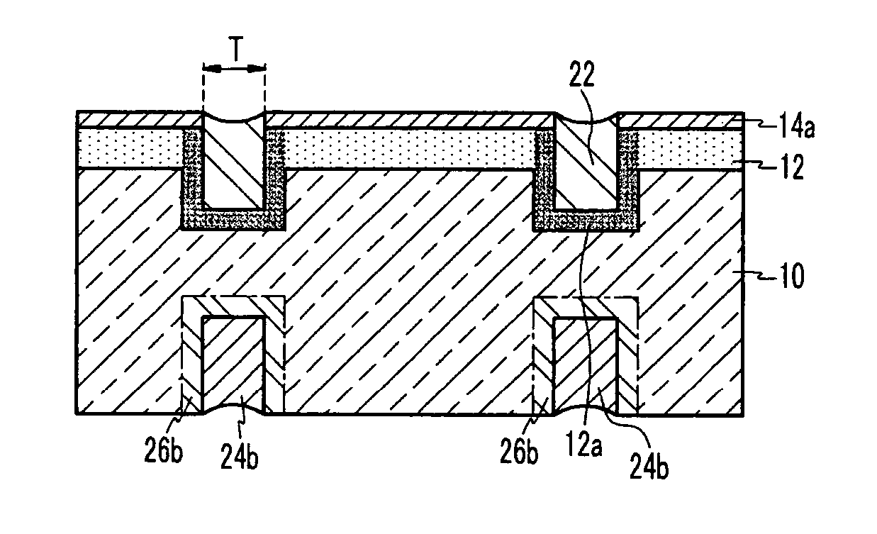
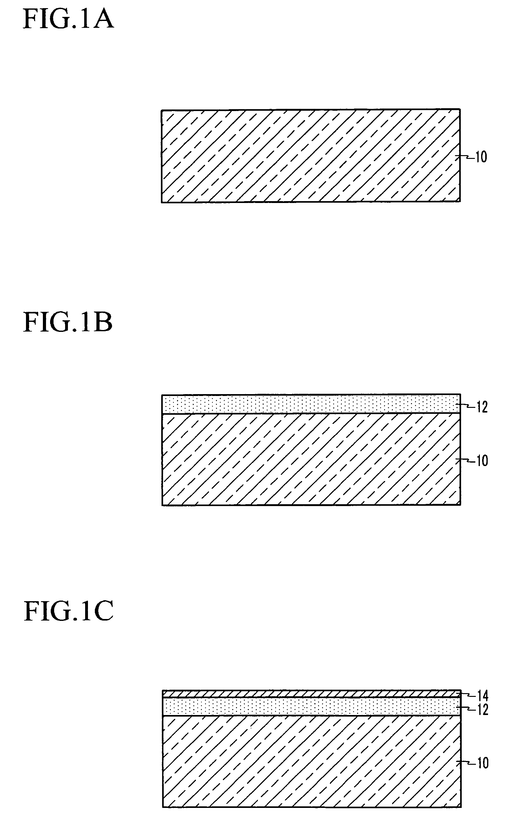
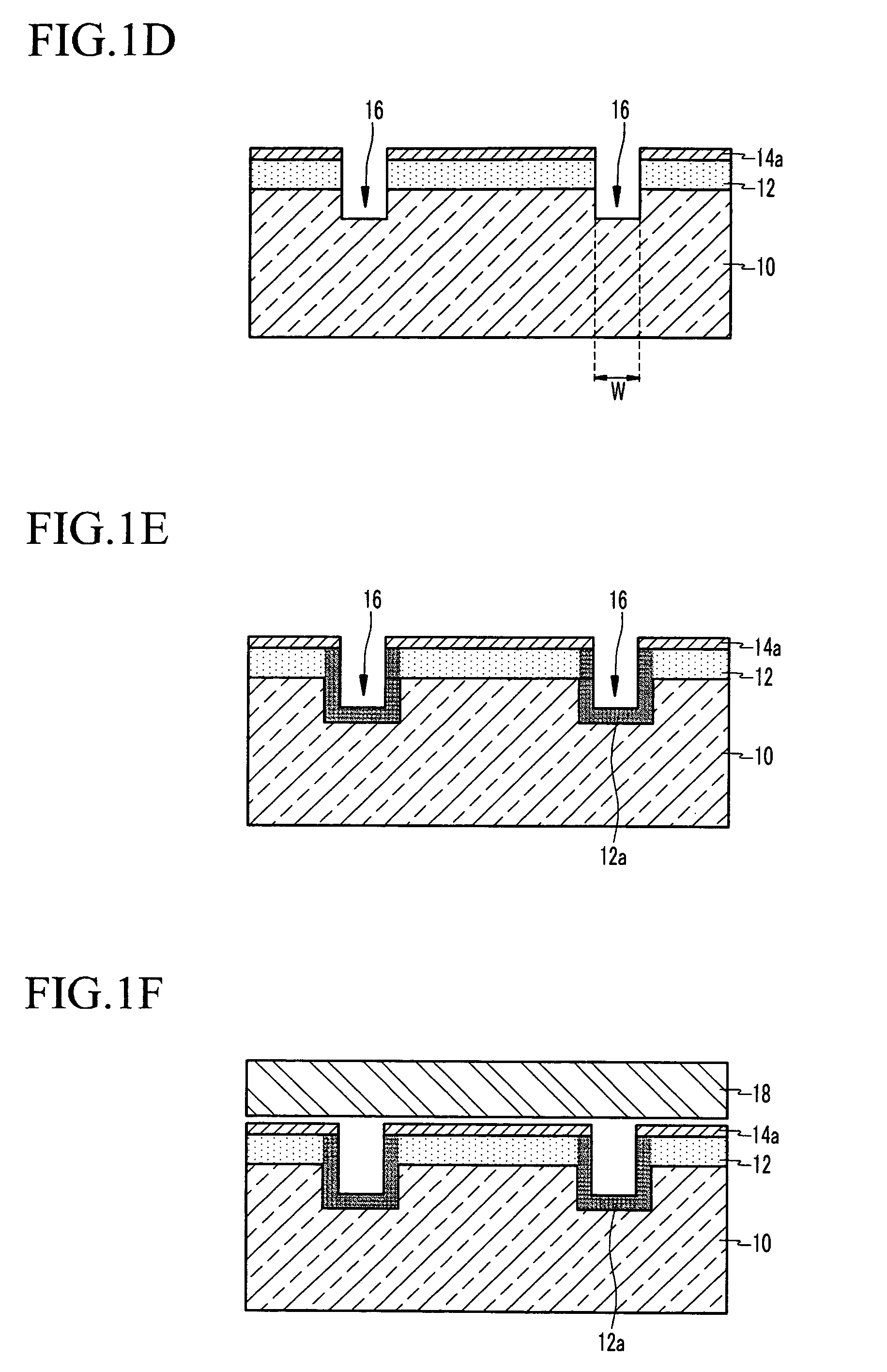
[0033]Hereinafter, a solar cell and a method of manufacturing the same according to an embodiment of the present invention will be described in detail with reference to the attached drawings such that the present invention can be easily put into practice by those skilled in the art.

[0034]FIGS. 1A thru 1J are cross-sectional views showing a method of manufacturing a solar cell according to an embodiment of the present invention.

[0035]First, as shown in FIG. 1A, a p-type semiconductor substrate 10 formed of silicon is prepared. However, the present invention is not limited thereto. That is, an n-type semiconductor substrate or a semiconductor substrate formed of various semiconductor materials except silicon may be used.

[0036]In order to improve the property of the solar cell, a preprocessing step may be performed. The preprocessing step is performed by etching the semiconductor substrate 10 using an alkali aqueous solution or a mixed acid solution, and removing impurities using a cle...


PUM


Abstract

A buried contact solar cell which is capable of operating with high efficiency is manufactured by a method which comprises the steps of forming a groove in a surface of a substrate, and forming an electrode by filling a conductive material in the groove using a laser. The step of forming the electrode may include positioning a conductive thin plate above the surface of the substrate, melting the conductive thin plate using a laser in a pattern corresponding to the groove, filling the conductive material in the groove, and removing the conductive thin plate.

Description

CLAIM OF PRIORITY[0001]This application makes reference to, incorporates the same herein, and claims all benefits accruing under 35 U.S.C.§119 from an application for SOLAR CELL AND METHOD OF MANUFACTURING THE SAME earlier filed in the Korean Intellectual Property Office on 6 Jan. 2006 and there duly assigned Ser. No. 10-2006-0001683.BACKGROUND OF THE INVENTION[0002]1. Field of the Invention[0003]The present invention relates to a solar cell and a method of manufacturing the same, and more particularly, to a buried contact solar cell capable of accomplishing high efficiency and a method of manufacturing the same.[0004]2. Description of the Related Art[0005]A solar cell generates electric energy using solar energy. The solar cell is eco-friendly and has an infinite energy source and a long life span. The solar cell can be a silicon solar cell and a dye-sensitized solar cell.[0006]The silicon solar cell includes a semiconductor substrate and an emitter layer that are of different cond...

Claims


Application Information

Patent Timeline
Patent Type & Authority Patents(United States)
IPC IPC(8): H01L21/00H01L31/00
CPCH01L31/022425Y02E10/50H01L31/04H01L31/0224H01L31/18
Inventor PARK, SANG-WOOK
Owner INTELLECTUAL KEYSTONE TECH LLC
Why Eureka
Try Eureka