
Nonvolatile memory cell array architecture for high speed reading

a memory cell array and high-speed reading technology, applied in the field of non-volatile semiconductor memory, can solve the problems of inability to perform random access in non-volatile semiconductor memories, inability to continuously output data, so as to increase the wiring width of each source line, prevent the increase of the chip size, and increase the size of the memory cell array without increasing the size of the memory cell array.

Inactive Publication Date: 2011-01-04
SOCIONEXT INC
View PDF16 Cites 4 Cited by
  • Summary
  • Abstract
  • Description
  • Claims
  • Application Information

AI Technical Summary

Benefits of technology

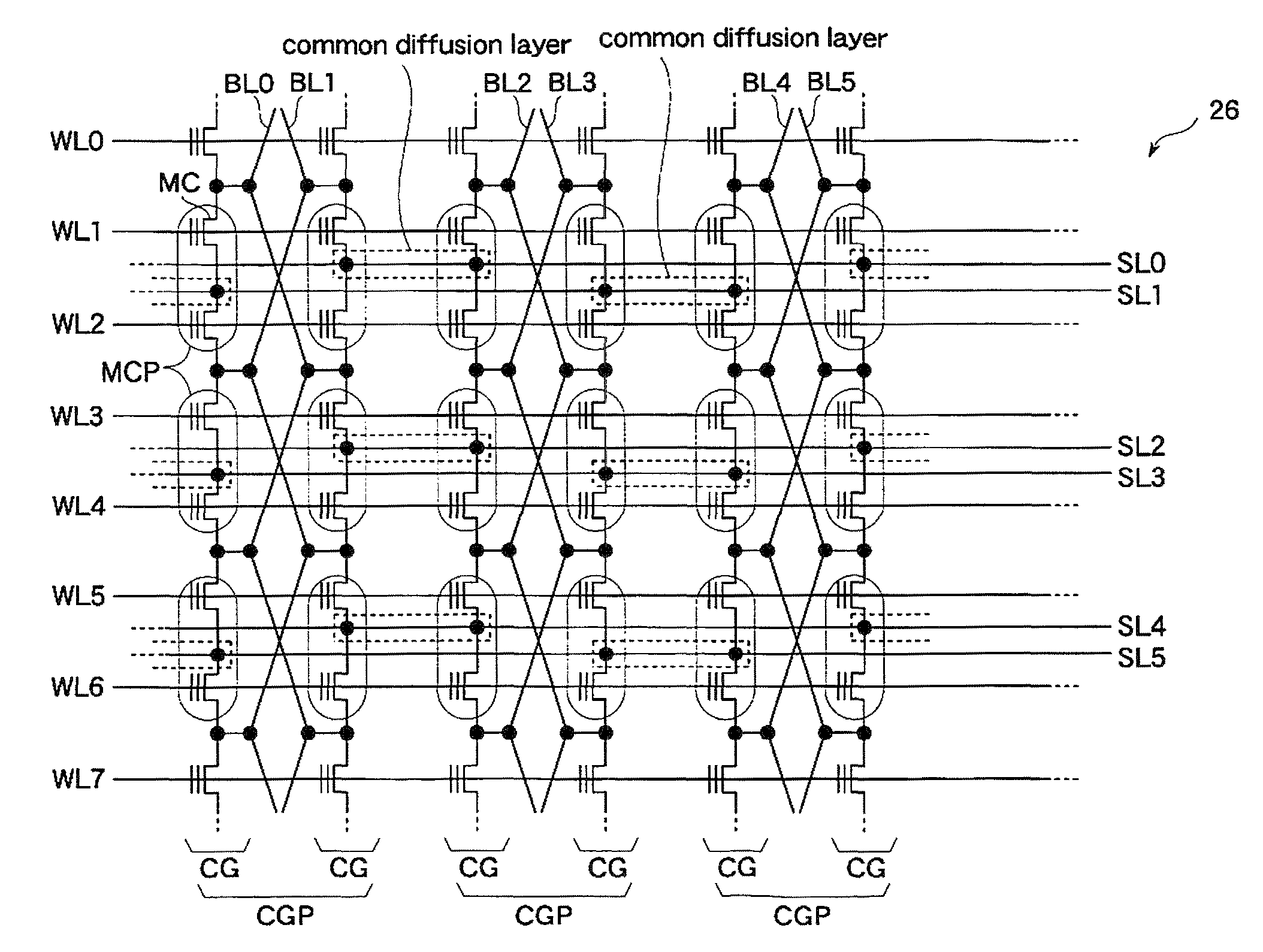
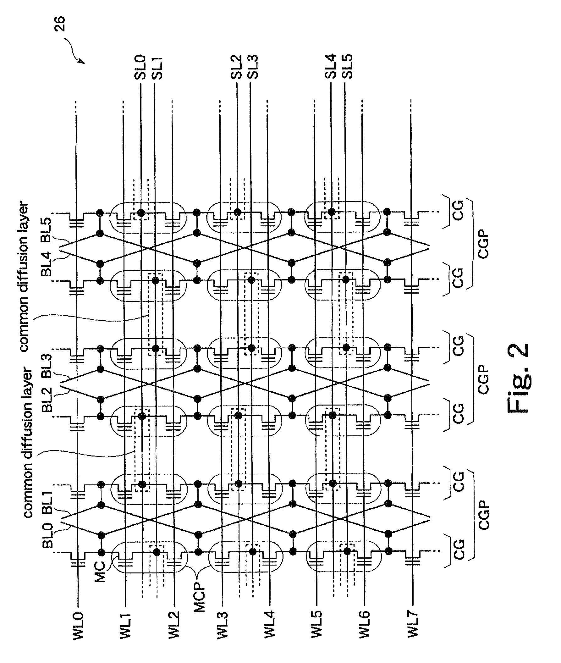
The present invention provides a nonvolatile semiconductor memory that allows for random access in a way that does not increase the chip size. The memory has a pipeline function for performing consecutive read operations in parallel, and multiple cell groups are arranged in a matrix form. The combination of bit lines and source lines is unique to each cell group, and a source decoder or column decoder sets the voltage of the corresponding line to a ground voltage or drain voltage, allowing for random access in a nonvolatile memory that performs plural read operations in parallel. The invention also includes a method for overlapping the activation periods of word lines to perform multiple read operations in parallel.

Problems solved by technology

Therefore, where addresses are supplied randomly (random access) in read operations, data cannot be output continuously from the memory cells.
That is, where random access is performed on one subarray, data cannot be output continuously.
In particular, random access cannot be performed in nonvolatile semiconductor memories in which parallel processing (pipeline processing) is performed by overlapping a part of activation periods of word lines in read operations.

Method used


Image

  • Nonvolatile memory cell array architecture for high speed reading
  • Nonvolatile memory cell array architecture for high speed reading
  • Nonvolatile memory cell array architecture for high speed reading

Examples


Embodiment Construction

An embodiment of the present invention will be hereinafter described with reference to the drawings. Double circles in the drawings mean external terminals. In the drawings, a signal line shown by a thick line is composed of plural lines. In the drawings, each of part of blocks to which the thick line(s) is connected is composed of plural circuits. A signal that is supplied via an external terminal is denoted by a symbol that is the same as the name of the terminal. A signal line that transmits a signal is given a symbol that is the same as the name of the signal.

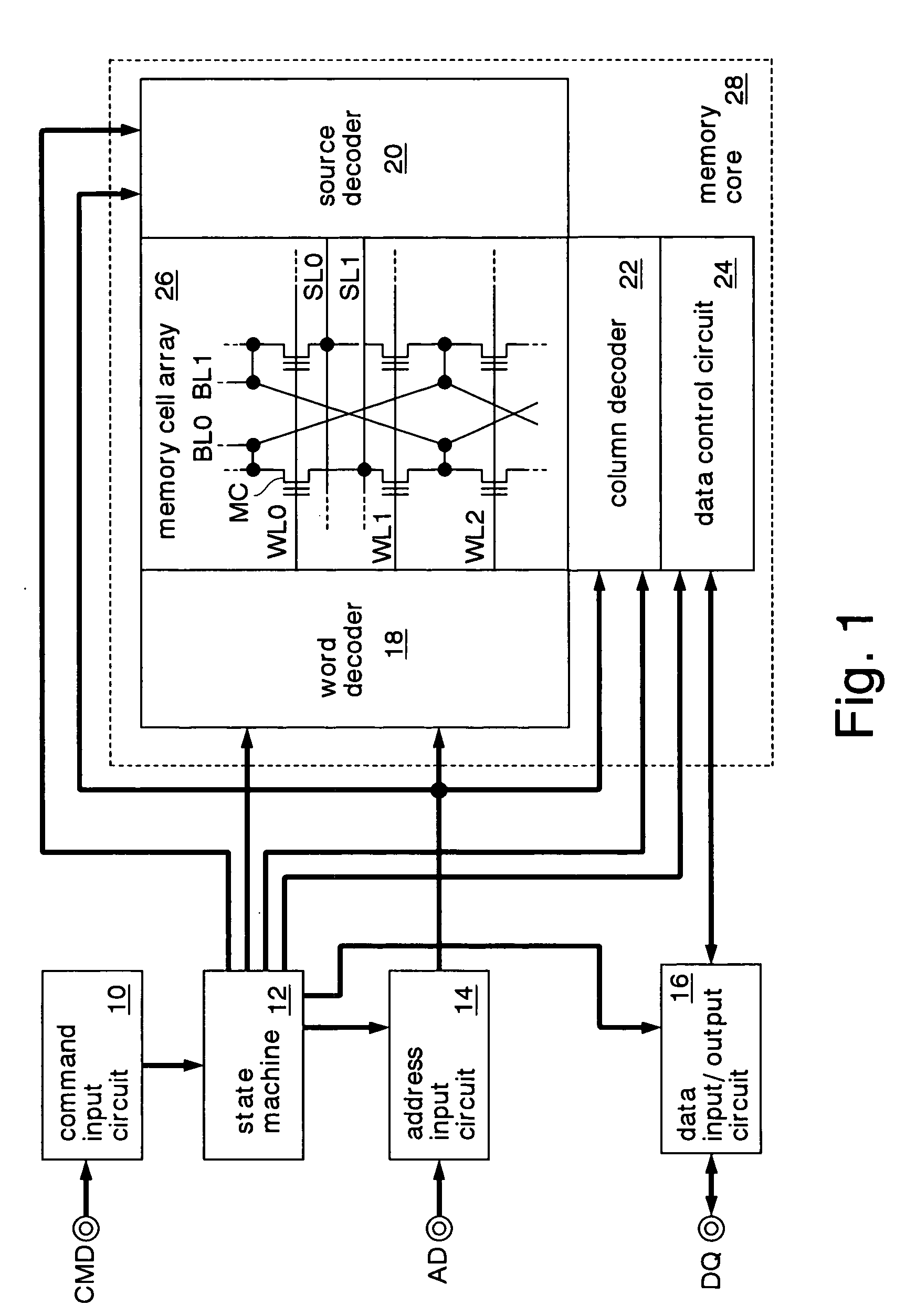
FIG. 1 shows a nonvolatile semiconductor memory according to an embodiment of the invention. This nonvolatile semiconductor memory is a NOR flash memory which is formed on a silicon substrate by a CMOS process. The flash memory has a command input circuit 10, a state machine 12, an address input circuit 14, a data input / output circuit 16, a word decoder 18, a source decoder 20, a column decoder 22, a data control circuit 24...


PUM


Abstract

When different word lines are accessed sequentially, to perform access operations in parallel, a word decoder overlaps a part of activation periods of those word lines. That is, a nonvolatile semiconductor memory is capable of pipeline processing for performing access operations in parallel. All the combinations of bit lines and source lines that are connected to the drains and the sources of nonvolatile memory cells are different from each other. Therefore, even when plural word lines are activated to perform plural read operations in parallel, a memory cell current is allowed to flow only between the drain and the source of a nonvolatile memory cell concerned. As a result, random access in which desired nonvolatile memory cells are accessed sequentially is enabled in a nonvolatile semiconductor memory having a pipeline function for performing plural read operations in parallel.

Description

BACKGROUND OF THE INVENTION1. Field of the InventionThe present invention relates to a nonvolatile semiconductor memory having nonvolatile memory cells.2. Description of the Related ArtNonvolatile semiconductor memories such as flash memories store data by holding or not holding electrons in the floating gates or trap gates of memory cell transistors (hereinafter also referred to as “memory cells”). For example, in a nonvolatile semiconductor memory disclosed in Japanese Unexamined Patent Application Publication No. 7-114796, memory cells are formed at the intersecting points of word lines and bit lines which are perpendicular to each other. Source lines which are connected to the sources of the memory cells are arranged parallel with the word lines. The sources of memory cells that are arranged along a pair of word lines are connected to a common source line. The drains of memory cells that are arranged parallel with the bit lines are connected to a common bit line.Japanese Unexami...

Claims


Application Information

Patent Timeline
Patent Type & Authority Patents(United States)
IPC IPC(8): G11C11/34G11C16/04
CPCG11C16/0416G11C16/26G11C16/32H01L27/115H10B69/00
Inventor IIOKA, OSAMU
Owner SOCIONEXT INC
Learn More