

Acene-based organic semiconductor materials and methods of preparing and using the same
a technology of organic semiconductor materials and organic semiconductors, applied in the direction of anthracene dyes, non-metal conductors, sustainable manufacturing/processing, etc., can solve the problems of poor solubility, poor air stability, and limit the type of manufacturing process (e.g. printing deposition) that can be used with n-type semiconducting compounds
- Summary
- Abstract
- Description
- Claims
- Application Information
AI Technical Summary
Problems solved by technology
Method used
Image

Examples
example 1
Synthesis of Organic Semiconductor Intermediates
A. Preparation of N-octylmaleimide
To a suspension of maleic anhydride (3.0 g, 30.6 mmol) in 80 mL of benzene, a solution of octylamine (3.59 g, 27.8 mmol) in 50 mL of benzene was added. The resulting mixture was stirred at 30° C. for an hour and zinc bromide (ZnBr2, 6.89 g, 30.6 mmol) and hexamethyl disilazane (6.72 g, 41.7 mmol) in 20 mL of benzene were added. The resulting suspension was heated under reflux for 2 hours. After cooling to room temperature, the reaction mixture was poured into 200 mL of 0.5 M hydrochloric acid (HCl). The organic layer was separated and the aqueous portion was extracted twice with 150 mL portions of ethyl acetate (EtOAc). The combined organic layers were washed with saturated aqueous sodium bicarbonate (NaHCO3, 2×150 mL), brine (1×150 mL), and dried over magnesium sulfate (MgSO4). The solution was concentrated under vacuum to yield a viscous solid, which is subsequently sublimed to produce N-octylmaleimi...
example 2
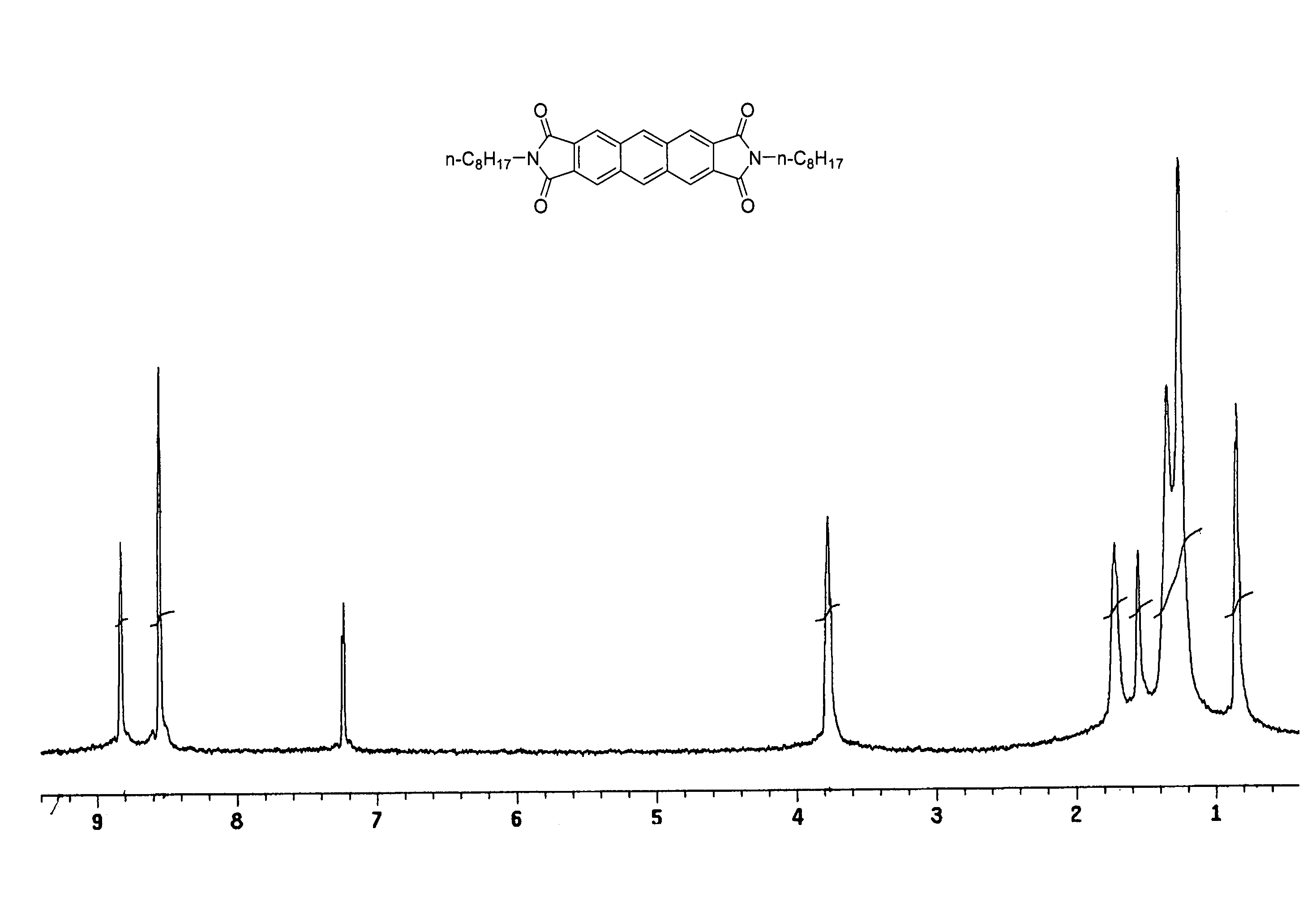
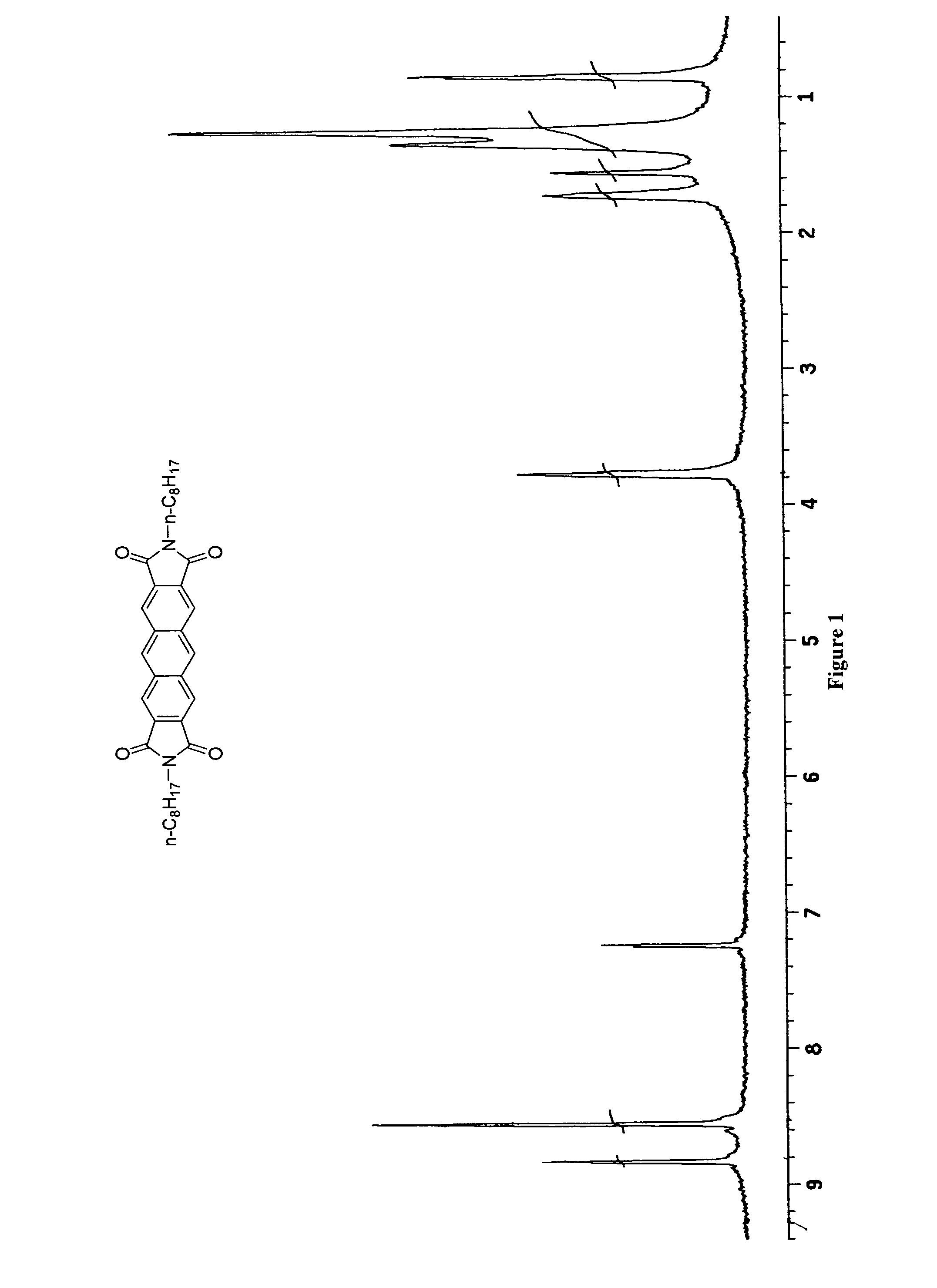
N,N′-Di-n-octyl-2,3:6,7-anthracenedicarboximide (ADI8)
Sodium iodide (NaI, 4.2 g) was added to a solution of 1,2,4,5-tetrakis(dibromomethyl)benzene (0.68 g, 0.89 mmol) and N-n-octylmaleimide (0.335 g, 1.79 mmol) in N,N-dimethylacetamide (10 mL). The mixture was heated at 80° C. for 12 hours during which time a precipitate formed. The precipitate was collected by filtration, washed with water and boiling dioxane to provide 0.40 g of N,N′-di-n-octyl-2,3:6,7-anthracenedicarboximide as a bright yellow solid (0.30 g, 0.55 mmol, 21% yield). Additional purification can be achieved by gradient sublimation. M.p.>300° C.; and Elemental Analysis (Calcd for C34H40N2O4: C, 75.53; H, 7.46; N, 5.18). found: C, 74.78; H, 7.10; N, 5.07.
FIG. 1 is 1H NMR spectra of N,N′-di-n-octyl-2,3:6,7-anthracenedicarboximide in deuterated chloroform (CDCl3).
example 3
N,N′-Dibenzyl-2,3:6,7-anthracenedicarboximide (ADI1Ph)
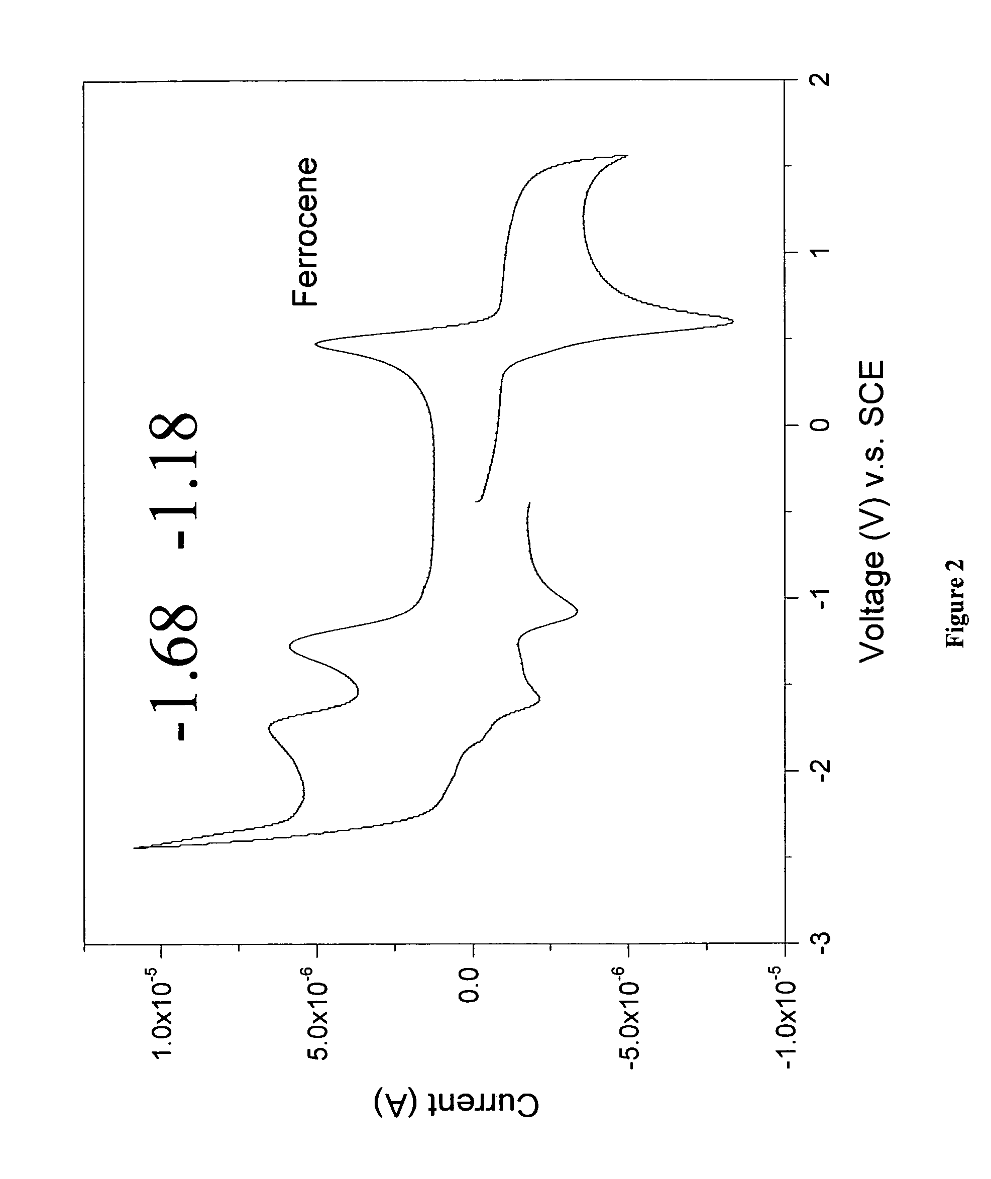
NaI (4.0 g) was added to a solution of 1,2,4,5-tetrakis(dibromomethyl)benzene (2.0 g, 2.61 mmol) and N-benzylmaleimide (0.977 g, 5.22 mmol) in N,N-dimethylacetamide (25 mL). The mixture was heated at 80° C. for 12 hours. The product was collected from the dark solution by filtration, and washed with water and boiling dioxane to provide 0.40 g of N,N′-dibenzyl-2,3:6,7-anthracenedicarboximide as a bright yellow solid (31% yield). Additional purification can be achieved by gradient sublimation. M.p.>300° C.; 1H NMR (400 MHz, DMSO-d6, 130° C.): δ 9.2 (s, 2H), 8.7 (s, 4H), 7.2-7.4 (m, 10H), 4.8 (s, 4H); and Elemental Analysis (Calcd for C32H20O4N2: C, 77.42; H, 4.03; N, 5.65). found: C, 77.25; H, 4.09; N, 5.69.
FIG. 2 is a cyclic voltammogram of N,N′-dibenzyl-2,3:6,7-anthracenedicarboximide in tetrahydrofuran using a carbon working electrode, a platinum counter electrode, and a silver wire pseudo-reference electrode. The electrolyte is...
PUM
| Property | Measurement | Unit |
|---|---|---|
| semiconductor | aaaaa | aaaaa |
| electron mobility | aaaaa | aaaaa |
| Rg | aaaaa | aaaaa |
Abstract
Description
Claims
Application Information