Semiconductor device and method for fabricating the same

a technology of semiconductors and semiconductors, applied in the direction of semiconductor devices, basic electric elements, electrical equipment, etc., can solve the problems of reducing reducing the breakdown resistance of devices, and deteriorating the breakdown resistance, so as to increase the distance between trenches, reduce the threshold voltage vt, and reduce the effect of breakdown resistan

Inactive Publication Date: 2011-03-01
PANASONIC CORP
View PDF7 Cites 11 Cited by
  • Summary
  • Abstract
  • Description
  • Claims
  • Application Information

AI Technical Summary

Benefits of technology

[0013]An object of the present invention is to provide a semiconductor device having a trench gate structure and a method for fabricating the same, in which even if the structure is miniaturized, the electric potential of the low concentration p-type body region is stabilized and breakdown resistance is increased, and at the same time, decrease of a threshold voltage Vt is suppressed.
[0015]Owing to this structure in which a distance between trenches of the source region is great, the electric potential of the low concentration body region located under the source region is not easily lowered even if the structure is miniaturized. As a result, a parasitic bipolar transistor is prevented from being turned on and resistance to breakdown that is caused by a surge voltage is increased. Moreover, decrease of a threshold voltage is suppressed and the degree of freedom of a control range of the threshold voltage is increased.
[0016]Further, by sandwiching a trench between the source region and the high concentration body region, resistance to breakdown that is caused by a surge voltage is increased even if the total area of the source region and the high concentration body region is equal to the total area of those of a conventional semiconductor device.
[0018]A trench according to this method has a concavo-convex shape when viewed from above. Hence, it is possible to increase a distance between trenches of the source region than a distance between trenches of the high concentration body region. As a result, it is possible to form a semiconductor device in which a low concentration body region is less likely to be influenced by a gate voltage and resistance to breakdown that is caused by the surge voltage is increased.
[0019]As explained, according to a semiconductor device of the present invention and a method for fabricating the same, it is possible to provide a semiconductor device having a trench gate structure in which, even if the structure is miniaturized, the electric potential of the low concentration body region is stabilized and breakdown resistance is increased, and at the same time, decrease of a threshold voltage Vt is suppressed.

Problems solved by technology

However, problems such as mentioned below will occur in the above structure if miniaturization proceeds and the distance between trenches is reduced.
If the parasitic bipolar transistor is turned on due to a surge voltage, the parasitic bipolar transistor generates heat and the current increases, which leads the device to thermal breakdown.
As a result, breakdown resistance is deteriorated.

Method used


Image

  • Semiconductor device and method for fabricating the same
  • Semiconductor device and method for fabricating the same
  • Semiconductor device and method for fabricating the same

Examples


embodiment 1

1. Structure of Semiconductor Device

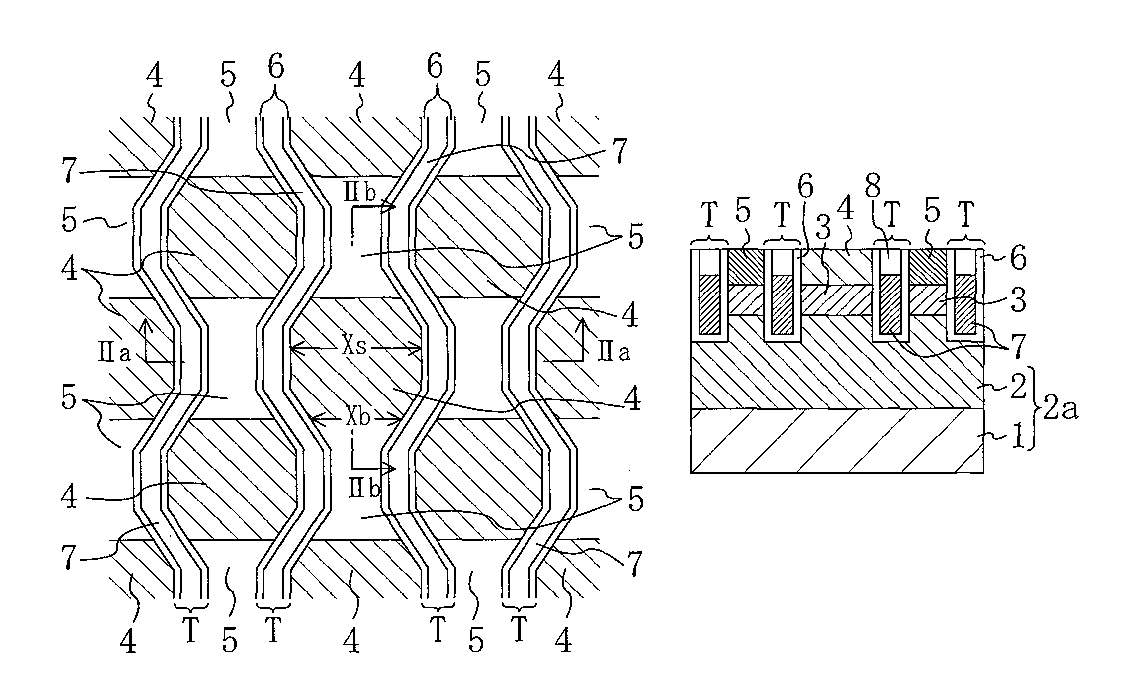
[0031]FIG. 1 is a plan view of a semiconductor device having a trench gate structure according to the first embodiment of the present invention. FIG. 2A and FIG. 2B show cross sections taken along the line IIa-IIa and the line IIb-IIb, respectively, of the semiconductor device of FIG. 1. The insulating film 8 shown in FIG. 2A is omitted from FIG. 1 for better viewing of the structure.

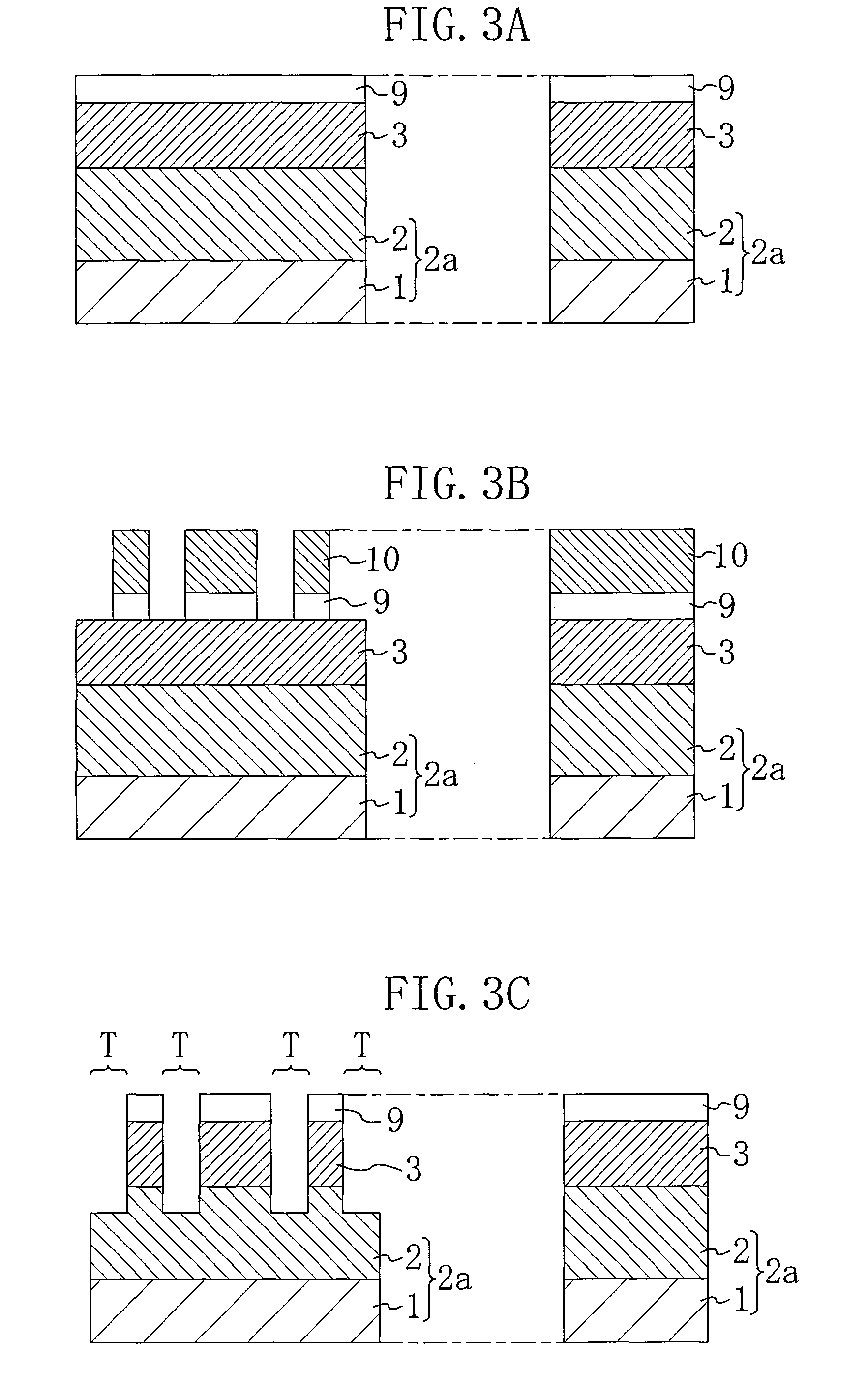
[0032]As shown in FIG. 1, FIG. 2A and FIG. 2B, a semiconductor device of the present embodiment includes: a low concentration p-type body region 3 formed on an n-type drain region 2a; an n-type source region 4 and a high concentration p-type body region 5, both being formed on the low concentration p-type body region 3; a plurality of trenches T each of which is formed from top faces of the n-type source region 4 and the high concentration p-type body region 5 and passes through the n-type source region 4, the high concentration p-type body region 5, and the low conce...

embodiment 2

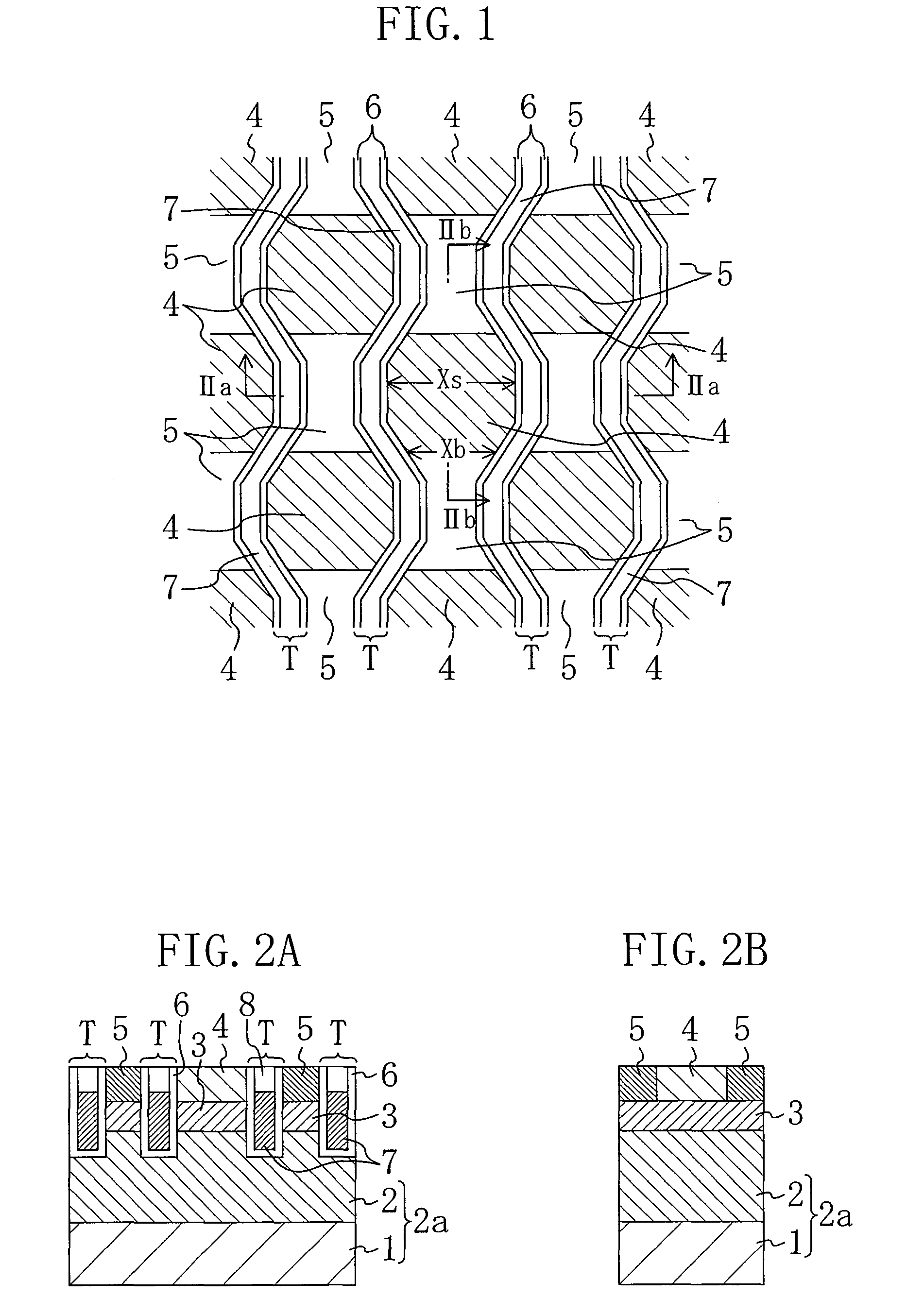
[0051]FIG. 8 is a plan view showing a semiconductor device according to the second embodiment of the present invention.

[0052]The semiconductor device of the first embodiment has a structure in which a trench T is sandwiched between an n-type source region 4 and a high concentration p-type body region 5. However, in the semiconductor device of the present embodiment, a trench T is composed of a part that is sandwiched between n-type source regions 4 and a part that is sandwiched between high concentration p-type body regions 5, and a maximum width of the part that is sandwiched between the n-type source regions 4 is narrower than a maximum width of the part that is sandwiched between the high concentration p-type body regions 5.

[0053]According to the semiconductor device of the present embodiment, the width of the gate electrode 7 at the part that is sandwiched between the n-type source regions 4 is narrower than the width of the gate electrode 7 of the semiconductor device of the fi...


PUM


Abstract

Disclosed is a semiconductor device having an n-type drain region, a low concentration p-type body region formed on the n-type drain region, an n-type source region formed on the low concentration p-type body region, a high concentration p-type body region formed on the low concentration p-type body region, a gate insulating film, and a gate electrode, wherein a plurality of trenches T which extend in a same direction and each of which forms a continuous concavo-convex shape when viewed from above are formed from top faces of the source region and the high concentration body region and pass through the low concentration body region to reach into the drain region, and wherein the gate electrode is buried in each of the plurality of trenches. A maximum distance between two adjacent trenches T of the n-type source region is greater than a maximum distance between the two adjacent trenches T of the high concentration p-type body region.

Description

BACKGROUND OF THE INVENTION[0001]1. Field of the Invention[0002]The present invention relates to a semiconductor device having a trench MOS (Metal Oxide Semiconductor) gate structure and a method for fabricating the same.[0003]2. Description of Related Art[0004]A trench MOS gate structure, in which a trench (groove) is formed in a semiconductor substrate and a gate oxide film and a gate electrode are formed in the trench, has been employed in semiconductor devices such as a power MOSFET (Field Effect Transistor) or the like and is widely used for a DC-DC converter, load switch, or the like of electronics equipment. With the recent trend of low power consumption and high speed of electronic equipment, demand for decrease in on-resistance of a MOSFET used in the equipment is growing.[0005]An example of a MOSFET which has a trench MOS gate structure designed for reducing on-resistance is disclosed, for example, in Japanese Laid-Open Patent Publication No. 2005-45123. FIG. 9A is a plan ...

Claims


Application Information

Patent Timeline
Patent Type & Authority Patents(United States)
IPC IPC(8): H01L21/336H01L29/76
CPCH01L29/4238H01L29/66734H01L29/7813H01L29/0696
Inventor TAKAMI, YOSHINORI
Owner PANASONIC CORP
Why Eureka
Try Eureka