Forced ion migration for chalcogenide phase change memory device

a phase change memory and chalcogenide technology, applied in semiconductor devices, digital storage, instruments, etc., can solve the problems of high programming current requirements, variation in switching voltage and on/off resistance ratio, thermal stress on materials, etc., to improve the phase-change memory response, increase the glass transition temperature, and improve the effect of phase-change memory respons

Active Publication Date: 2011-04-12
BOISE STATE UNIVERSITY
View PDF110 Cites 36 Cited by
  • Summary
  • Abstract
  • Description
  • Claims
  • Application Information

AI Technical Summary

Benefits of technology

[0011]One possible benefit of the metal-chalcogenide layer is the potential for formation of an Ohmic contact between the electrode and the memory layer due to the presence of a low bandgap material like SnTe (Eg=0.18 eV at 300K [see Esaki, L.; Stiles, P. J. “New Type of Negative Resistance in Barrier Tunneling”Phys. Rev. Lett. 16 (1966) 1108-1111]) between the electrode and the chalcogenide switching layer. An Ohmic contact will allow a lower voltage to be applied to the memory cell since a Schottky barrier does not need to be overcome in order to achieve the current necessary for phase-change switching. Another potential benefit of the Sn-chalcogenide layer is better adhesion of the memory layer to the electrode. The better adhesion provided by the SnTe layer may help prevent delamination of the electrode from the chalcogenide memory layer, as can occur after repeated thermal cycles [see Hudgens, S.; Johnson, B. “Overview of Phase-Change Chalcogenide Nonvolatile memory Technology”MRS Bulletin, November 2004, 829-832]. In addition to these potential benefits, the Sn-chalcogenide may provide a region with ‘graded’ chalcogenide concentration between the Sn-chalcogenide and the Ge-chalcogenide memory switching layer due to the ability of the chalcogenide to form bridging bonds between the Sn and Ge atoms in the Sn-chalcogenide and Ge-chalcogenide layers, respectively. Lastly, as we show in this work, the Sn-chalcogenide material may assist in phase-change memory switching by donating Sn-ions to the Ge-chalcogenide layer during operation, thus allowing chalcogenide materials which normally do not exhibit phase change memory switching to be chemically altered post processing into an alloy capable of phase change response.

Problems solved by technology

“A 0.18-um 3.0-V 64-Mb nonvolatile phase-transition random access memory (PRAM)”IEEE J Solid-State Circuits 40 (2005) 293-300] but there have been many challenges to the implementation of a phase-change memory product such as the high programming current requirements, variation in switching voltages and ON / OFF resistance ratios, thermal stresses on the materials, and their adhesion to the electrodes.

Method used


Image

  • Forced ion migration for chalcogenide phase change memory device
  • Forced ion migration for chalcogenide phase change memory device
  • Forced ion migration for chalcogenide phase change memory device

Examples


Embodiment Construction

[0024]Referring to the Figures, there are shown some, but not the only, embodiments of the invention.

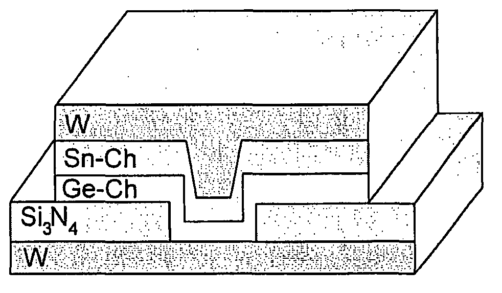
[0025]FIG. 3 shows a top perspective view of a device structure, according to the present invention, used in this study. The device structure consists of a via through a nitride layer to a W bottom electrode deposited on 200 mm p-type Si wafers. The chalcogenide material layers were deposited with the Ge-chalcogenide layer first, followed by the Sn-chalcogenide layer. Prior to deposition of the first chalcogenide layer, the wafers received an Ar+ sputter etch to remove residual material and any oxide layer that may have formed on the W electrode. The Ge2Se3 layer was deposited by sputtering with an Ulvac ZX-1000 from a target composed of pressed Ge2Se3 powder. The GeTe, SnTe, and SnSe layers were prepared by thermal evaporation of GeTe, SnTe, and SnSe (all from Alfa Aesar, 99.999% purity) using a CHA Industries SE-600-RAP thermal evaporator equipped with three 200 mm wafer planetary ...


PUM


Abstract

Non-volatile memory devices with two stacked layers of chalcogenide materials comprising the active memory device have been investigated for their potential as phase change memories. The devices tested included GeTe / SnTe, Ge2Se3 / SnTe, and Ge2Se3 / SnSe stacks. All devices exhibited resistance switching behavior. The polarity of the applied voltage with respect to the SnTe or SnSe layer was critical to the memory switching properties, due to the electric field induced movement of either Sn or Te into the Ge-chalcogenide layer. One embodiment of the invention is a device comprising a stack of chalcogenide-containing layers which exhibit phase change switching only after a reverse polarity voltage potential is applied across the stack causing ion movement into an adjacent layer and thus “activating” the device to act as a phase change random access memory device or a reconfigurable electronics device when the applied voltage potential is returned to the normal polarity. Another embodiment of the invention is a device that is capable of exhibiting more that two data states.

Description

[0001]This application claims priority of my prior provisional patent application, Ser. 60 / 853,068, filed on Oct. 19, 2006, entitled “Forced Ion Migration for Chalcogenide Phase Change Memory Device,” which is incorporated herein by reference.[0002]This work was partially supported by a NASA Idaho EPSCoR grant, NASA grant NCC5-577.BACKGROUND OF THE INVENTION[0003]1. Field of the Invention[0004]This invention relates generally to electronic memory devices, and more particularly to a method of inducing a non-phase change stack structure into a phase change stack memory structure.[0005]2. Related Art[0006]Research into new random access electronic memory technologies has grown significantly in the past 10 years due to the near realization of the scaling limits of DRAM and the low cycle lifetime, high power requirements, and radiation sensitivity of Flash. At the forefront of this research is the phase-change random access memory (PCRAM) [see Bez, R.; Pirovano, A. “Non-volatile memory t...

Claims


Application Information

Patent Timeline
Patent Type & Authority Patents(United States)
IPC IPC(8): G11C11/00
CPCH01L45/06H01L45/1233H01L45/143H01L45/1625H01L45/1641H01L45/1683H01L45/144Y10S977/754H10N70/8825H10N70/231H10N70/041H10N70/026H10N70/8828H10N70/826H10N70/066
Inventor CAMPBELL, KRISTY A.
Owner BOISE STATE UNIVERSITY
Why Eureka
Try Eureka