Embedded phase noise measurement system
a phase noise and measurement system technology, applied in pulse manipulation, instruments, pulse techniques, etc., can solve the problems of reducing the predictive power of the phase noise equation, attenuating amplitude noise, and rf and microwave sources exhibiting some amount of frequency instability
- Summary
- Abstract
- Description
- Claims
- Application Information
AI Technical Summary
Benefits of technology
Problems solved by technology
Method used
Image
Examples
examples
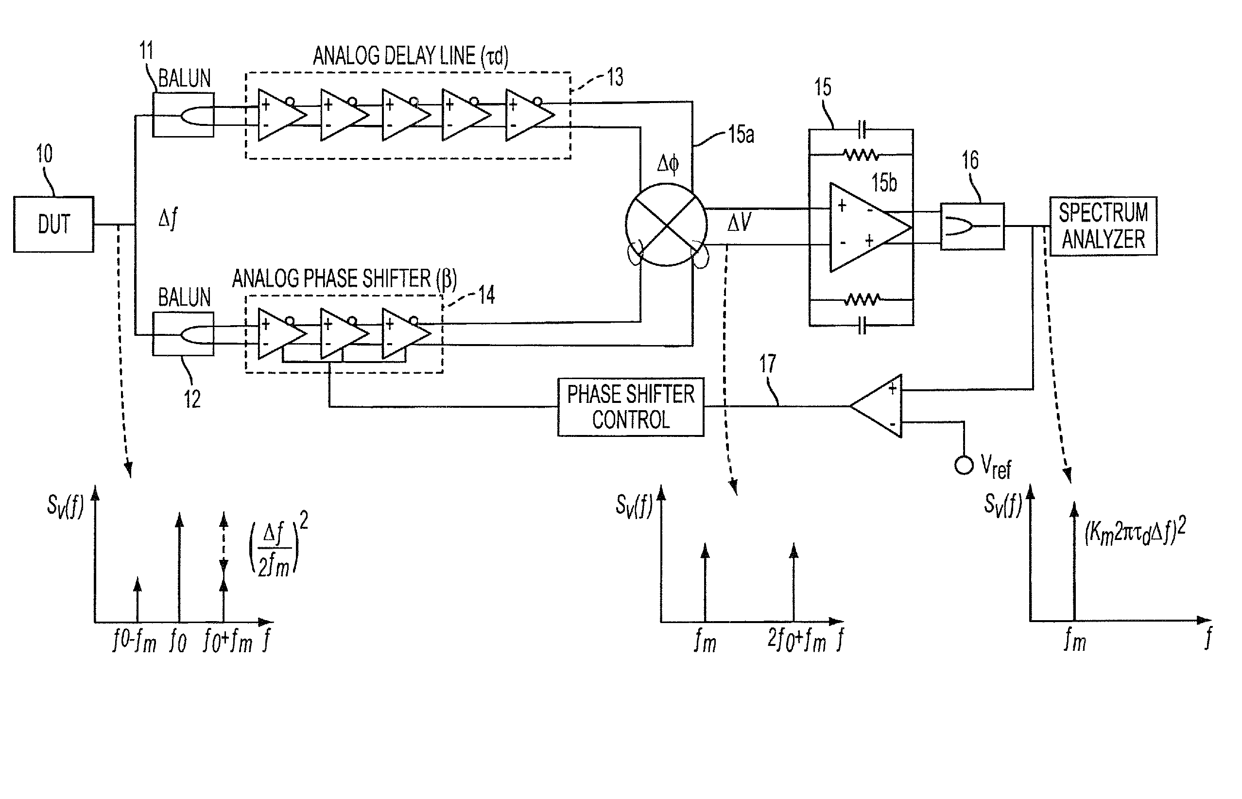
[0181]A phase noise measurement circuit was fabricated in a 0.13 μm, seven metal CMOS process (IBM8HP) as described in the 2009 Thesis by Jaeshin Kim entitled “Broadband Balun and Phase Noise Measurement System Design for RFIC Testing.” The fabricated noise measurement circuit occupied an active area of 1 mm×15 mm. For the example test design, the active baluns are self-biased by using a biasing resistor at the input port. The active delay line uses three dc biases: VDCIN (≅0.4V) for the input dc level. VCDLY (0.5˜1.2V) for the current source biasing of the active delay line to control the active delay line gain, and VBDLY (0.35˜0.6 V) for the current source biasing of a source follower of the dc level shifter. Depending on the carrier frequency, the active delay line gain will vary. Thus, the current source biasing controls the active delay line gain. In addition, by controlling the source follower current, the fine tuning of an active delay line gain can be possible.
[0182]The phas...
PUM
 Abstract
Description
Claims
Application Information


