Memory element comprising an organic compound and an insulator

a technology of organic compound and memory element, applied in the field of memory element, can solve the problems of reducing the reliability of a memory device and a semiconductor device, data cannot be rewritten, and short-circuiting between the electrodes, so as to prevent short-circuit in an initial state, reduce the amount of applied voltage and current in writing data in the memory element, and reduce the amount of applied current. effect of applied voltage and current amoun

Inactive Publication Date: 2011-06-07
SEMICON ENERGY LAB CO LTD
View PDF42 Cites 13 Cited by
  • Summary
  • Abstract
  • Description
  • Claims
  • Application Information

AI Technical Summary

Benefits of technology

[0006]In view of the foregoing problems, it is an object of the present invention to provide a nonvolatile memory element, in which data can be written once other than in manufacturing and forgery and the like due to rewriting can be prevented, a memory device including the memory element, and a semiconductor device including the memory device. It is another object of the present invention to provide a memory device and a semiconductor device, which are highly reliable and inexpensive.
[0017]According to the present invention, it is possible to obtain a semiconductor device, in which data can be written once other than in manufacturing a chip and forgery and the like due to rewriting can be prevented. Further, by providing an insulating layer with a thickness of 4 nm or less, and preferably, 2 nm or less between a conductive layer and an organic compound layer to be in contact with the conductive layer, tunnel current flows through the insulating layer, and therefore, variations in applied voltage and amount of current in writing data in the memory element can be reduced. Further, by providing the insulating layer with a thickness of 4 nm or less, and preferably, 2 nm or less, between the conductive layer and the organic compound layer to be in contact with the conductive layer, a charge injecting property of the memory element is increased due to a tunnel effect, and a thickness of the organic compound layer can be increased, thereby making it possible to prevent short-circuiting in an initial state. As a consequence, reliability of the memory device and the semiconductor device can be improved. Furthermore, each of the memory device and the semiconductor device of the present invention includes the memory element having a simple structure in which the organic compound layer is interposed between the pair of conductive layers, and therefore, the memory device and the semiconductor device are less expensive.

Problems solved by technology

A mask ROM has a simple structure; however, it is necessary to write data during a manufacturing process, and data cannot be rewritten.
Meanwhile, when a thickness of an organic compound layer is reduced to reduce writing voltage, short-circuiting may be caused between the electrodes in an initial state.
This may result in reduction of reliability of a memory device and a semiconductor device.

Method used


Image

  • Memory element comprising an organic compound and an insulator
  • Memory element comprising an organic compound and an insulator
  • Memory element comprising an organic compound and an insulator

Examples


embodiment mode 1

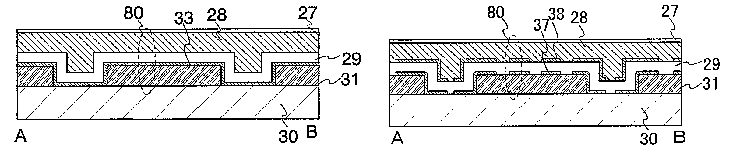
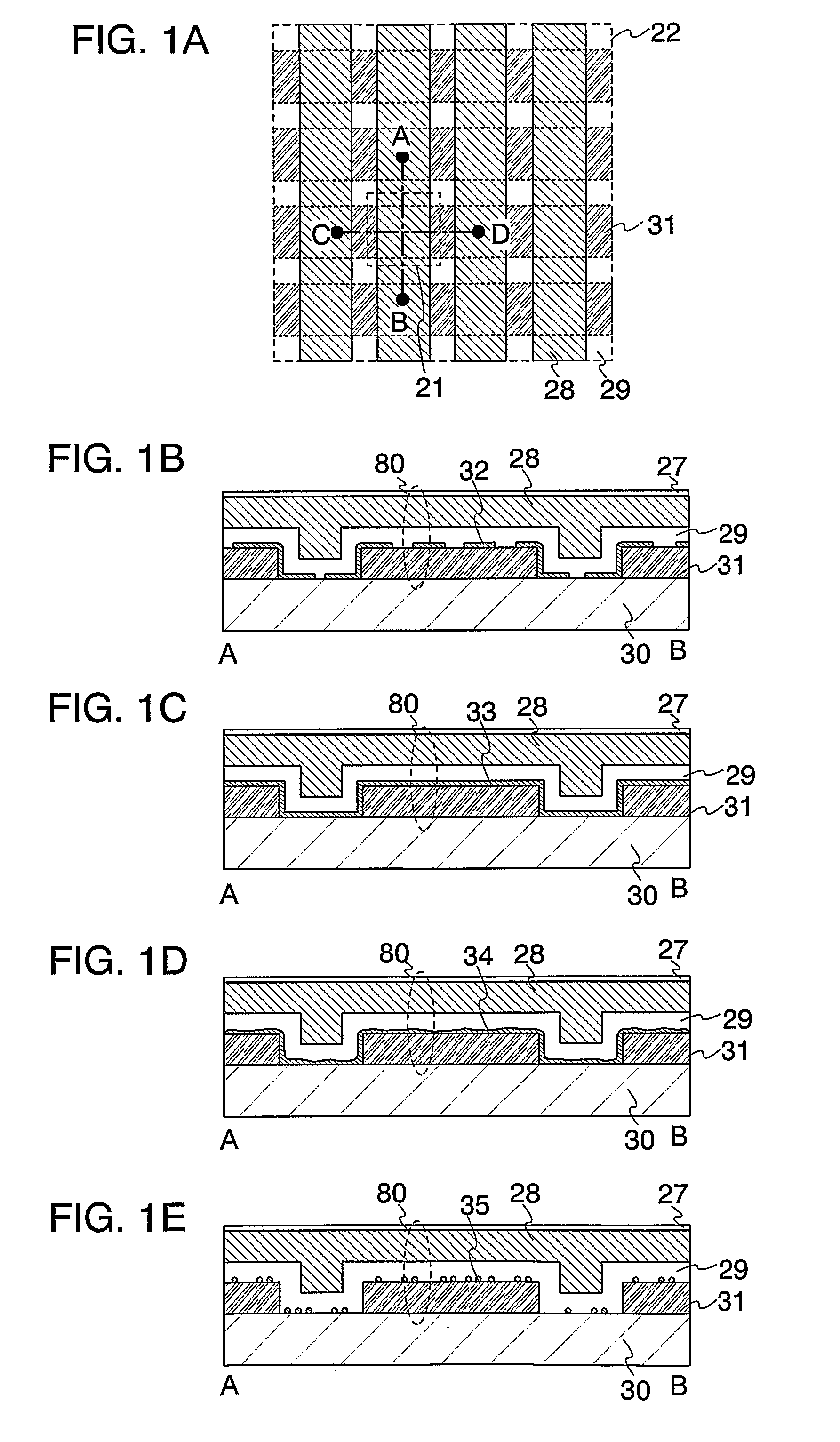
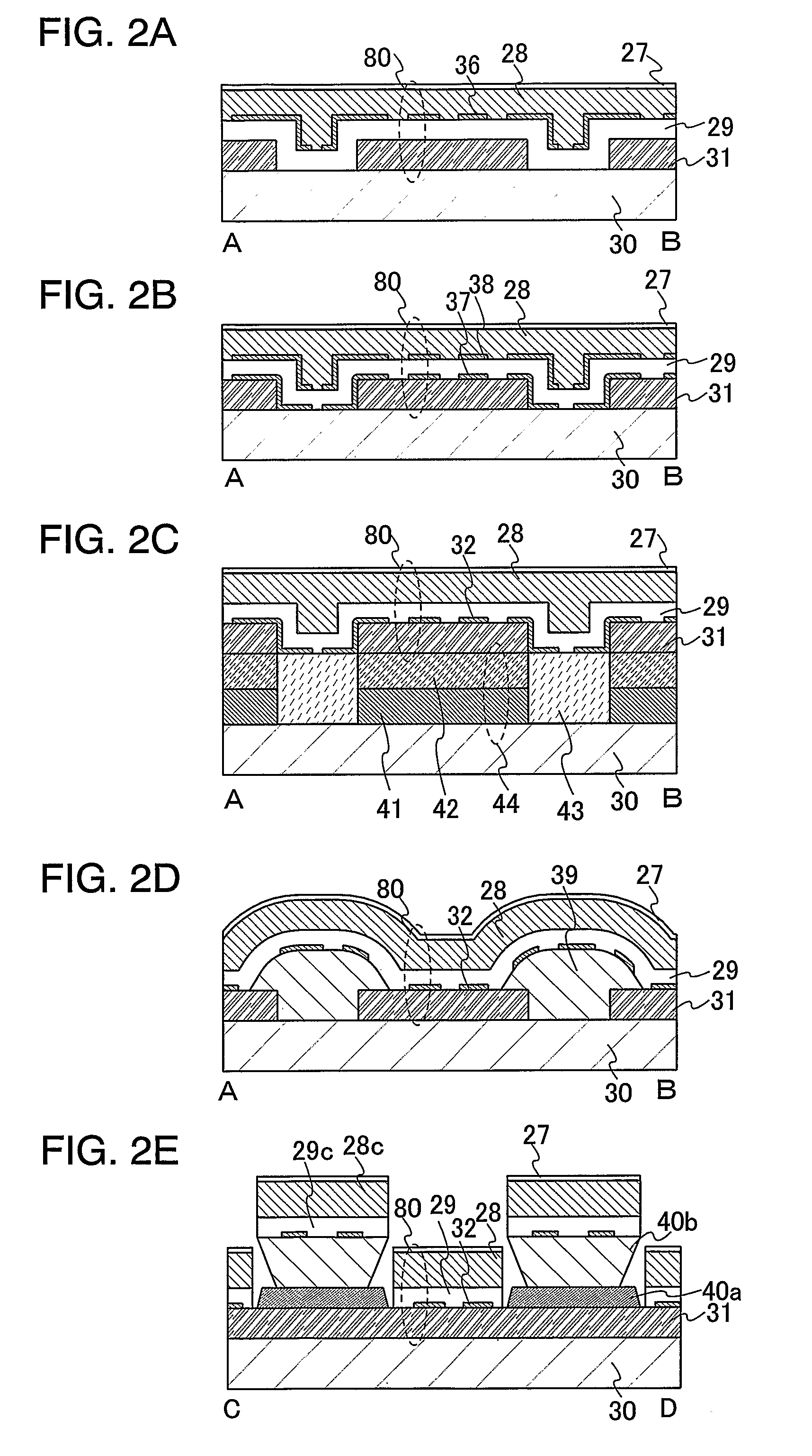
[0046]In this embodiment mode, structural examples of a memory element included in a memory device of the present invention will be described with reference to the drawings. Specifically, examples of a memory device having a passive matrix type structure will be shown.

[0047]FIG. 5A shows one structural example of an organic memory (a memory circuit 16) of this embodiment mode. The memory circuit 16 includes a memory array 22 in which memory cells 21 are arranged in a matrix form, a bit line driver circuit 26 having a column decoder 26a, a readout circuit 26b, and a selector 26c, a word line driver circuit 24 having a row decoder 24a and a level shifter 24b, and an interface 23 having a write circuit and the like and communicating with an external portion. Note that the structure of the memory circuit 16 shown in FIG. 5A is just one example; and therefore, the memory circuit may further include other circuit such as a sense amplifier, an output circuit, and a buffer, or, a write circ...

embodiment mode 2

[0105]In this embodiment mode, a memory device having a different structure from those of Embodiment Mode 1, will be described. Specifically, the memory device has an active matrix type structure.

[0106]FIG. 6A shows a structural example of an organic memory shown in this embodiment mode. The organic memory includes a memory cell array 222 in which memory cells 221 are arranged in a matrix form, a bit line driver circuit 226 having a column decoder 226a, a readout circuit 226b, and a selector 226c, a word line driver circuit 224 having a row decoder 224a and a level shifter 224b, and an interface 223 having a write circuit and the like and communicating with an external portion. Note that the structure of the memory circuit 216 shown in FIG. 6A is just one example; and therefore, the memory circuit may further include other circuit such as a sense amplifier, an output circuit, and a buffer, or, a write circuit may be provided in the bit line driver circuit.

[0107]Each of the memory ce...

embodiment mode 3

[0160]In this embodiment mode, an example of a semiconductor device having a memory device as shown in the above described embodiment modes, will be described with reference to the drawings.

[0161]One feature of the semiconductor device shown in this embodiment mode is that data can be read out from and written in the semiconductor device without contact. Data transmitting types can be largely classified into three of an electromagnetic coupling type in which a pair of coils are placed to face each other and communication is performed by mutual induction; an electromagnetic induction type in which communication is performed by an induction field; and a radio wave type in which communication is performed by utilizing radio waves. Any type can be employed. Further, there are two types of layouts of an antenna used for transmitting data: one is a case where an antenna is provided over a substrate over which a transistor and a memory element are provided; and the other is a case where a ...


PUM

PropertyMeasurementUnit
thicknessaaaaaaaaaa
thicknessaaaaaaaaaa
diameteraaaaaaaaaa

Abstract

On object of the invention is to provide a non-volatile memory device, in which data can be added to the memory device after a manufacturing process and forgery and the like by rewriting can be prevented, and a semiconductor device including the memory device. Another object of the invention is to provide a highly-reliable, inexpensive, and nonvolatile memory device and a semiconductor device including the memory device. A memory element includes a first conductive layer, a second conductive layer, a first insulating layer with a thickness of 0.1 nm or more and 4 nm or less being in contact with the first conductive layer, and an organic compound layer interposed between the first conductive layer, the first insulating layer, and the second conductive layer.

Description

TECHNICAL FIELD[0001]The present invention relates to a memory element, a memory device including the memory element, and a semiconductor device including the memory element.BACKGROUND ART[0002]In recent years, a semiconductor device having various functions, in which a plurality of circuits are integrated over an insulated surface, has been developed. Moreover, a semiconductor device which can conduct wireless transmission / reception of data by providing an antenna has been developed. Such a semiconductor device is referred to as a wireless chip (also referred to as an ID tag, an IC tag, an IC chip, a RF (Radio Frequency) tag, a wireless tag, an electronic tag, or a RFID (radio frequency identification)) tag, and has already brought to part of the market.[0003]Many of these semiconductor devices that have already been put into practical use have a circuit (also referred to as an IC (integrated circuit) chip) using a semiconductor substrate such as an Si substrate and an antenna, and...

Claims


Application Information

Patent Timeline
Patent Type & Authority Patents(United States)
IPC IPC(8): H01L29/08H01L35/24H01L51/00
CPCB82Y10/00G11C13/0069H01L27/101H01L27/112H01L27/11206H01L27/11286H01L27/1214H01L27/13H01L27/285G11C13/0014H01L51/0533G11C2013/009G11C2213/77G11C2213/79H01L27/105H01L27/12H01L51/0042H01L51/0051H01L51/0059H01L51/0081H01L27/1255H01L27/124H10B20/60H10B20/20H10B20/00H10K19/202H10K85/146H10K85/611H10K85/631H10K85/324H10K10/476H01L27/10G11C11/22H10K99/00
Inventor YUKAWA, MIKIOOHSAWA, NOBUHARUASAMI, YOSHINOBU
Owner SEMICON ENERGY LAB CO LTD
Why Eureka
Try Eureka