Method and system for improved phase noise in a BiCMOS clock driver

a clock driver and phase noise technology, applied in the field of clock driver methods and systems, can solve problems such as limited speed, large errors, poor phase noise,

Active Publication Date: 2011-06-28
ANALOG DEVICES INT UNLTD
View PDF26 Cites 3 Cited by
  • Summary
  • Abstract
  • Description
  • Claims
  • Application Information

AI Technical Summary

Problems solved by technology

Otherwise, the uncertainty in the timing of the sampling operation may create errors that are larger than that created in a quantizing process.
However, hardly any signal sources for low-phase noise signals, whether a quartz crystal oscillator, a resonant oscillator, or a carrier transmitting a signal through a medium, can deliver true rail-to-rail CMOS logic levels.
Therefore, a problem arises when translating a low-phase noise signal from low-levels such as ECL or a small sinusoid waveform to CMOS logic levels.
Unfortunately, such prior solutions have generally yielded poor phase noise, limited speed, excessive usage of power, or combinations thereof.
The capacitive loading of MOSFET gates in the '726 patent either limits the speed at which a circuit can operate, or requires substantial power to drive the gates.
Depending on the implementation, the solution proposed by the '726 patent may increase the noise level.
Thus, when combined with the inevitable slew-rate limitations, it creates timing uncertainties.
However, the performance of the circuit disclosed therein still can not produce desired phase noise performance because the noise level yielded from the PMOSFET (having its gate connected to its drain) is still too high.
This limits the available voltage swing, which subsequently degrades the signal to noise ratio.
Although the '580 patent represents an improvement over the '726 patent, the noise is still too large and leads to degradation of phase noise because of the current noise and the slew rate limiting that occurs.
Driving the gates with such current sources may result in acceptable speeds, but noise performance often suffers because of the noise present in the current sources.
Although the circuitry disclosed in the '746 patent provides some desirable features in some cases, the dynamic range of a current source based on a band-gap reference, which is defined as the quiescent current level divided by the current noise level, is often a limitation in achieving the most demanding phase noise performance.
The first is that the gate driven signals are still limited by the quiescent currents in the stage.
Thus, as passive devices, such MOSFETs do not increase the current available to drive the inverter gate terminals.
The second limitation is that the gate-to-drain connection of those MOSFETs inherently limits the signal to noise ratio, as previously discussed.
This substantial bias level has all the usual undesirable outcomes, including increased power consumption from the supply rails, increased heat generation on the chip.
It also causes an increase of the noise in the circuit because the base current noise of the NPN works into the pull-up resistor, R4 (110) which is substantially larger than the reciprocal of the transconductance (gm).
However, the time base noise is dominated by the noise of the current source on the edge that turns on the PMOS device.
The use of NMOS could introduce problems associated with the Vgs(ON) variability, particularly due to the bulk effect whereby the Vgs(ON) changes as a function on bulk voltage.
However, circuit 200 will result in a slight skew of the duty cycle at both outputs.
However, the skew occurs at the outputs due to the fact that the rising edge of either output is actively pulled by the PMOS devices and the falling edge will lag by approximately one inverter delay.
In that case, the noise level rises anyway due to base current noise flowing through the resistors which creates noise on the base nodes.

Method used


Image

  • Method and system for improved phase noise in a BiCMOS clock driver
  • Method and system for improved phase noise in a BiCMOS clock driver
  • Method and system for improved phase noise in a BiCMOS clock driver

Examples


Embodiment Construction

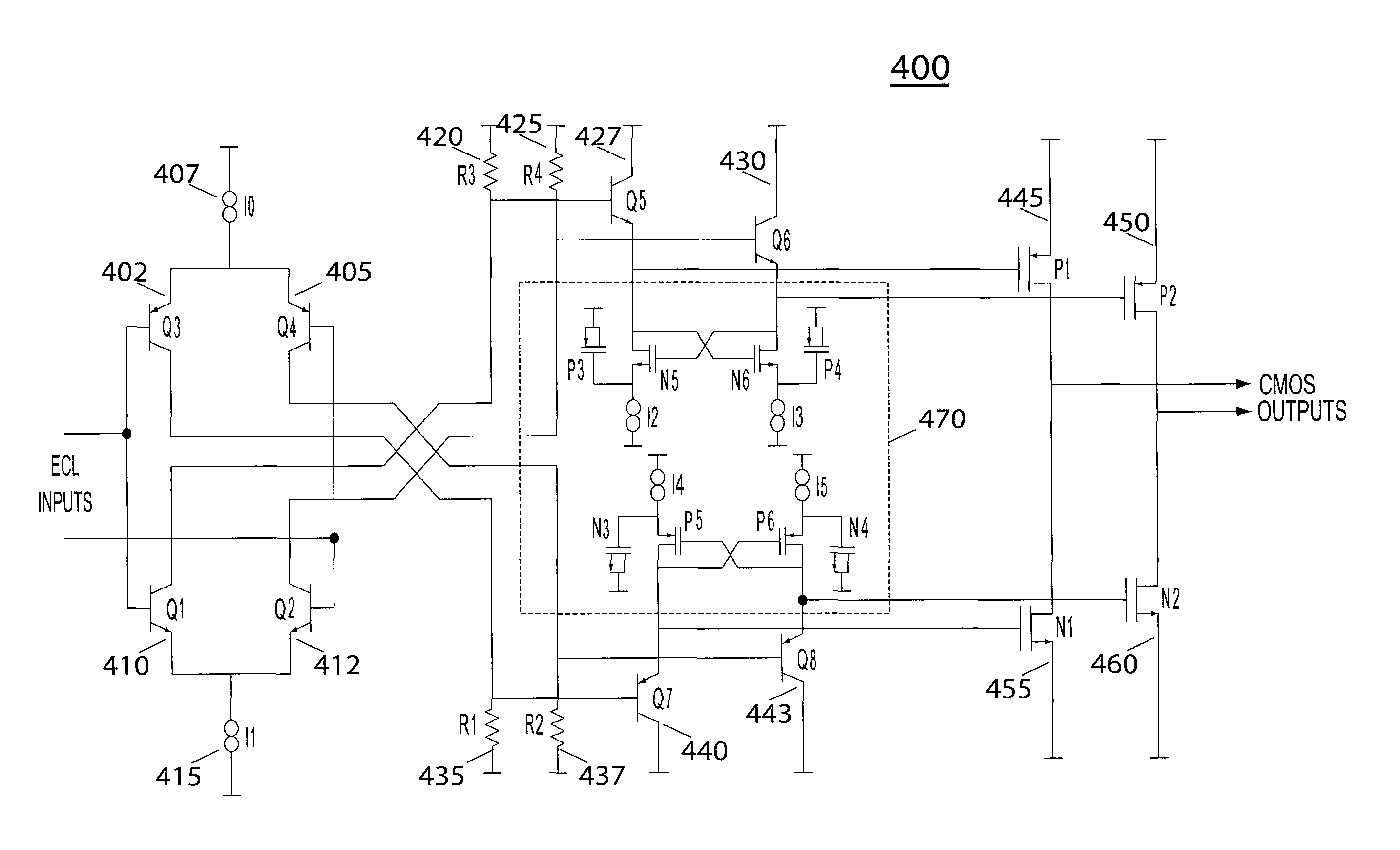
[0033]The present teaching relates to clock driver circuitry in general. More specifically, the present teaching relates to a BiCMOS clock driver circuitry to improve the phase noise performance of the clock driver.

[0034]The present teaching discloses a circuit suitable for use as a clock driver with reduced phase noise compared with each of the above prior art circuits. The improvement is achieved at the interface between the Bipolar (ECL) section and the CMOS section by actively driving the first MOSFET gates both up and down. In some embodiments, one direction is driven by a BJT emitter follower, while the other direction is driven by using a MOSFET switch to shuffle charge stored on a dummy MOSFET gate. It is understood that other embodiments are also possible in accordance with the scope as recited in the claims.

[0035]FIG. 4 shows an exemplary embodiment of a fully differential and complementary circuit 400 for driving a set of MOSFET gate terminals from conventional ECL logic,...


PUM


Abstract

System and method for a clock driver. An input taking circuit is used for receiving small-signal logic inputs. A voltage follower circuit is coupled to the input taking circuit and used to generate a set of voltage follower outputs. An output circuit is coupled to the voltage follower circuit to receive the set of voltage follower outputs as inputs and generate output signals. The voltage follower circuit is coupled to a switching circuit, that is connected to the set of voltage follower outputs and is deployed for reducing the phase noise level of the output signals.

Description

BACKGROUND[0001]1. Technical Field[0002]The present teaching relates to a method and system for clock driver and systems incorporating the same. More specifically, the present teaching relates to a method and system for a BiCMOS clock driver and systems incorporating the same.[0003]2. Discussion of Technical Background[0004]Modern signal processing systems frequently digitize and process high speed signals that have a wide dynamic range. Digitization includes both quantizing a signal into discrete levels, e.g., into 2n levels, in an n-bit Analog-to-Digital converter (ADC), as well as sampling a signal at discrete time intervals. Some high speed input signals are at a frequency higher than the sampling rate of the ADC used. This yields a condition called under-sampling, under which a precise repetitive time-based reference is needed. Otherwise, the uncertainty in the timing of the sampling operation may create errors that are larger than that created in a quantizing process. This wel...

Claims


Application Information

Patent Timeline
Patent Type & Authority Patents(United States)
IPC IPC(8): H03K19/094
CPCH03K3/013H03K3/021H03K19/017527H03K19/00346H03K19/01707H03K3/35613
Inventor PETROFSKY, JOSEPH GERARD
Owner ANALOG DEVICES INT UNLTD
Why Eureka
Try Eureka