
Semiconductor light-emitting material with tetrahedral structure formed therein

a technology of tetrahedral structure and semiconductor material, which is applied in the direction of semiconductor lasers, luminescent compositions, chemistry apparatus and processes, etc., can solve the problems of unsuitable optical field application of silicon, and theoretically impossible for silicon light emitting devices based on these techniques to emit light at high efficiency and high speed

Inactive Publication Date: 2011-07-12
KK TOSHIBA
View PDF2 Cites 1 Cited by
  • Summary
  • Abstract
  • Description
  • Claims
  • Application Information

AI Technical Summary

Benefits of technology

The present invention provides a semiconductor light-emitting material that has a tetrahedral structure formed by bonded atoms. The material includes a matrix semiconductor and impurity atoms that are bonded through charge transfer. The material is stretched in a direction of a bond. The invention also provides a light emitting device that includes an active layer made of the semiconductor light-emitting material and electrodes for supplying a current to the active layer. The technical effects of the invention include improved light-emitting efficiency and stability of the semiconductor material.

Problems solved by technology

Silicon, which is a typical electronic material supporting electronics, has been considered unsuitable for application in the optical field.
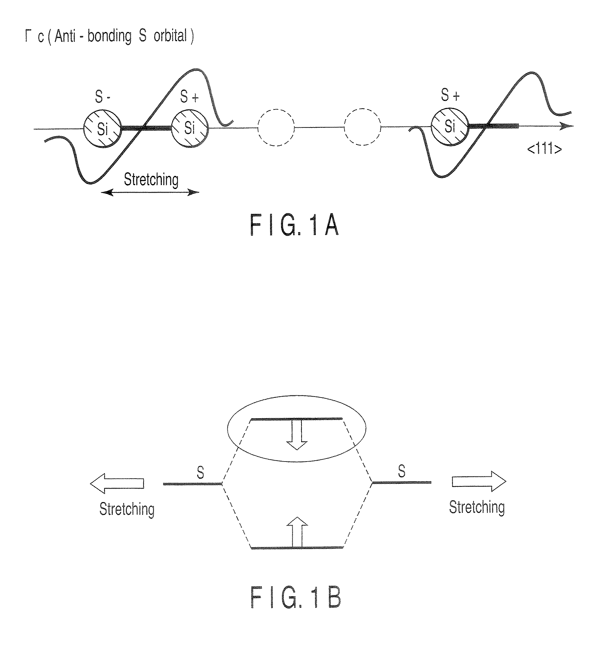
This is because silicon is of an indirect transition type and the conduction band and valence band of silicon are p-orbital (odd function), making silicon unsuitable for application in the optical field.
It is theoretically impossible for the silicon light emitting device based on these techniques to emit light at high efficiency and high speed.
Therefore, it is not expected intense emission using only any one of the effects.
Therefore, it has been impossible for the conventional silicon light-emitting device to exhibit sufficient characteristics and to be put into a practical use.
In the case of utilizing the confinement effect which has been considered most hopeful, a serious problem resides in that it is unavoidable to introduce a high electronic barrier.
It is difficult to inject a current over the high electronic barrier, so that the electroluminescence (EL) by the current injection method is inhibited.
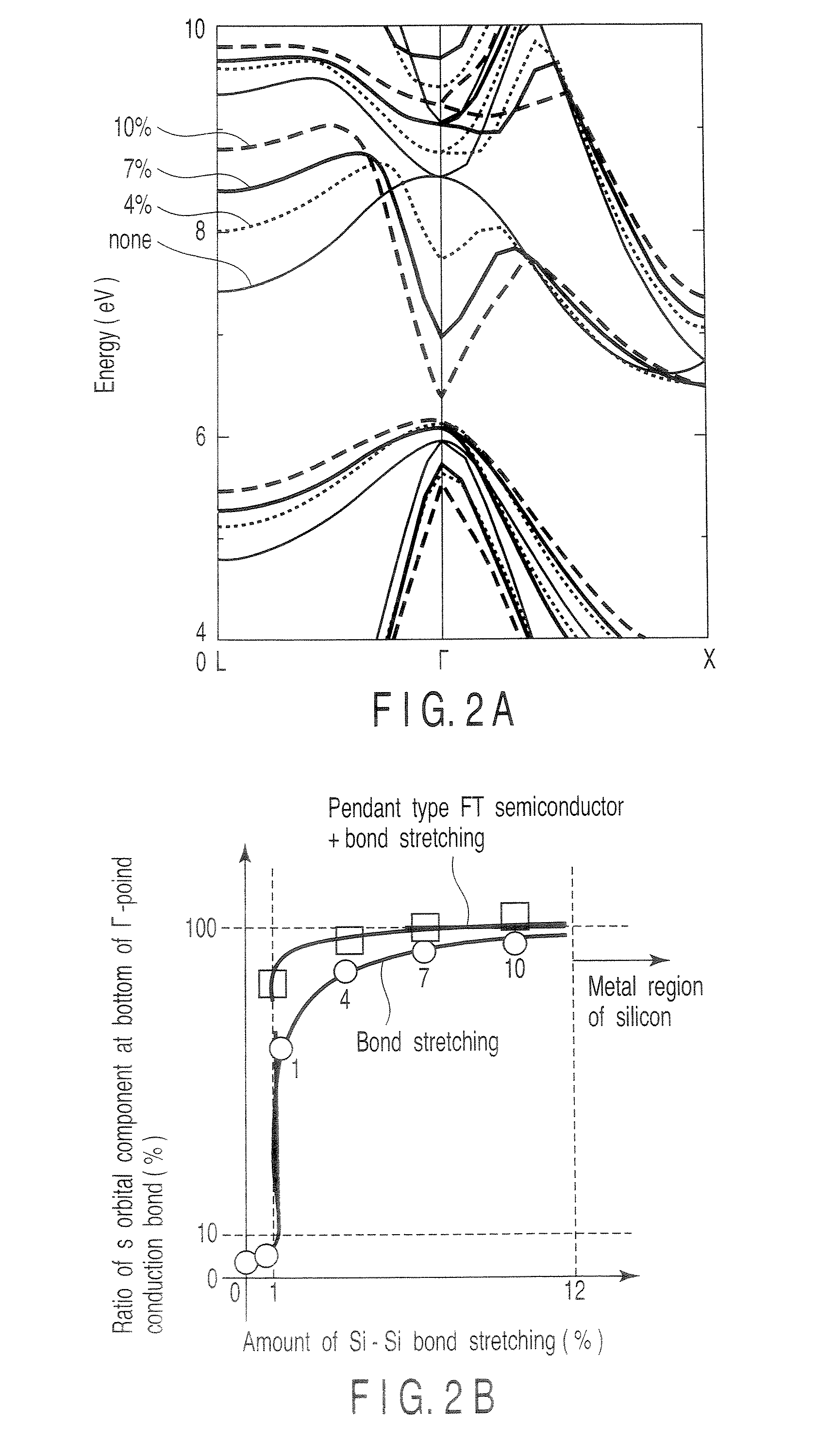
However, the document does not show at all to the modulation of the Γ-point relating to the improvement in the emission efficiency of the indirect semiconductor.
It follows that the FT semiconductor containing a rare gas is expected to be low in thermal stability and, thus, to be impracticable.
However, even if carbon is converted into a material of a direct transition type, a light emitting device having high efficiency and operated at high speed cannot be expected if the amount of the s-orbital component of the conduction band remains to be small.
Further, the discussion given in the document covers the case where uniaxial strain as high as 4% is introduced into a very hard carbon, which is impossible to achieve actually.
As described above, conventional techniques have a serious problem that it is impossible to modulate sufficiently the band structure of an indirect semiconductor, e.g., silicon.
Since an orbital component cannot be changed, it is impossible to use effectively a matrix component of dipole moment.
Also, in the case of utilizing the confinement effect, the electrons will be confined by a high electronic barrier, leading unavoidably to a problem that current injection is made difficult.

Method used


Image

  • Semiconductor light-emitting material with tetrahedral structure formed therein
  • Semiconductor light-emitting material with tetrahedral structure formed therein
  • Semiconductor light-emitting material with tetrahedral structure formed therein

Examples


first embodiment

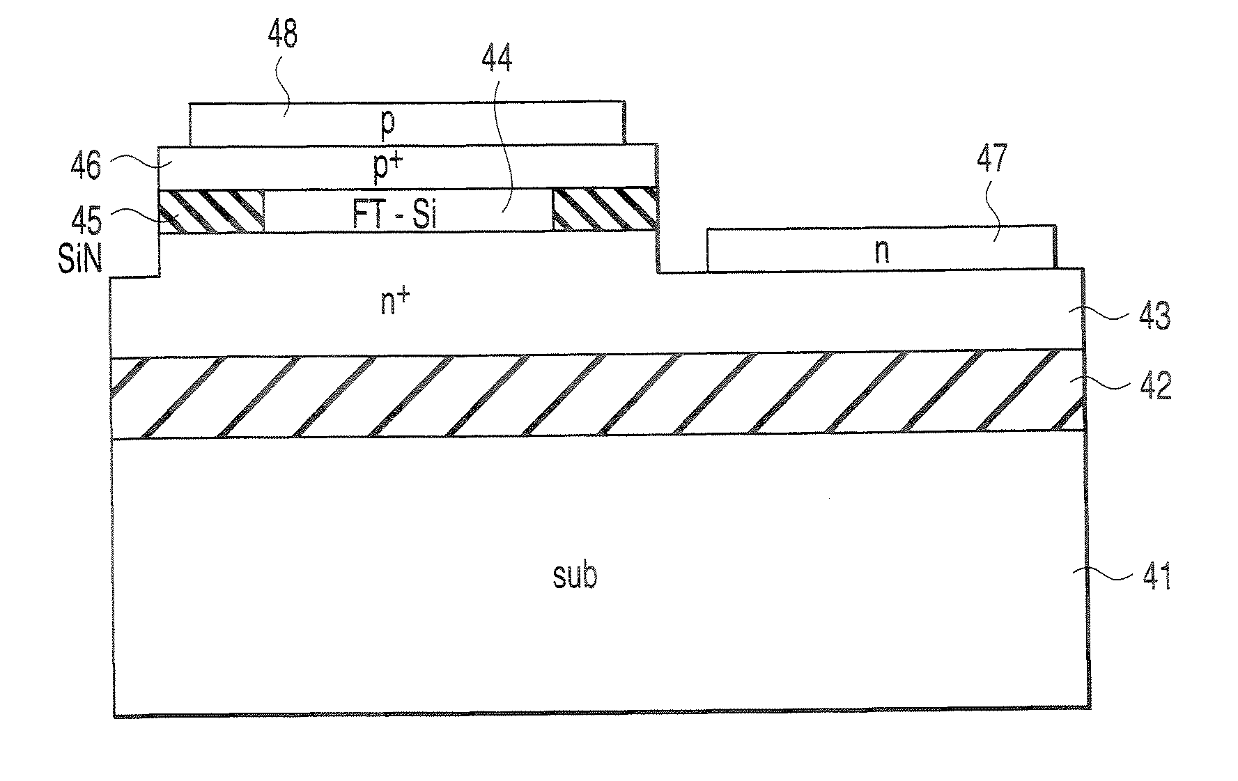
[0125]In this embodiment, a vertical type silicon light emitting device shown in FIG. 6A in which bond stretching is introduced in the active layer will be described. The n+ layer 1 is formed on a (111) silicon substrate (not shown). Then, the active layer 2 formed on the n+ layer 1 is patterned, followed by burying the SiN layer 3 in the region surrounding the active layer 2. By performing a thermal process, compressive stress is applied to the active layer 2 from the SiN layer 3 so that the active layer 2 is stretched in the direction, i.e., in the normal direction to the film plane. It can be confirmed by Raman spectroscopy that about several percent of bond stretching is introduced in the direction. Then, the p+ layer 4 is formed on the active layer 2. In order to forcedly inject a current into the active layer 2, it is desirable to use a metal with a small work function for the n-electrode. In this case, a SrSi electrode is used as an example.

[0126]EL emission can be observed...

second embodiment

[0133]In this embodiment, a vertical type silicon light emitting device shown in FIG. 6A in which bond stretching is introduced in the active layer comprising FT-Si will be described. The light emitting device in this embodiment can be manufactured by processes similar to those in the first embodiment except for the method of forming the active layer. The method of forming the active layer will be described below. Phosphorus atoms (P) used as the heteroatom S substituted for a lattice site of silicon, and fluorine atoms (F) used as the heteroatom I inserted into an interstitial site are ion-implanted simultaneously into the active layer. Each of the P concentration and the F concentration is about 2.5×10²⁰ / cm3. When the active layer is annealed at about 500° C. for a short time, the P atoms are substituted for lattice sites and the F atoms are inserted into interstitial sites adjacent to the P atoms at the lattice sites, so that stable PF pairs are formed. Whether the PF pair in the...

third embodiment

[0138]In this embodiment, a vertical type silicon light emitting device shown in FIG. 6A in which bond stretching is introduced in the active layer comprising FT-Si will be described. The light emitting device in this embodiment can be manufactured by processes similar to those in the second embodiment, except that another FT-Si is used as the material for the active layer. The method of forming the active layer will be described below. Indium atoms (In) are used as the heteroatom S substituted for a lattice site of silicon, and sodium atoms (Na) are used as the heteroatom I inserted into an interstitial site. Each of the In concentration and the Na concentration is about 5×10²⁰ / cm3 and the InNa pair concentration is about 5×10²⁰ / cm3. Whether the InNa pair in the pendant type FT structure is formed in the active layer can be confirmed by microscopic infrared spectroscopy. The natural vibration mode of the InNa pair appears in the vicinity of 140 to 180 cm−1.

[0139]Also, the SiN layer...


PUM


Abstract

A semiconductor light-emitting material includes a semiconductor substance including a matrix semiconductor whose constituent atoms are bonded to form a tetrahedral structure, an impurity atom S substituted for an atom in a lattice site of the matrix semiconductor, and an impurity atom I inserted in a interstitial site of the matrix semiconductor, the impurity atom S and the impurity atom I being bonded through charge transfer therebetween in a state that the impurity atom S has an electric charge coincident with that of the constituent atom of the matrix semiconductor and the impurity atom I has an electron configuration of a closed shell structure, in which the semiconductor substance is stretched in a direction of a bond forming the tetrahedral structure.

Description

CROSS-REFERENCE TO RELATED APPLICATIONS[0001]This application is based upon and claims the benefit of priority from prior Japanese Patent Application No. 2005-370250, filed Dec. 22, 2005, the entire contents of which are incorporated herein by reference.BACKGROUND OF THE INVENTION[0002]1. Field of the Invention[0003]The present invention relates to a semiconductor light-emitting material and a light emitting device.[0004]2. Description of the Related Art[0005]Silicon, which is a typical electronic material supporting electronics, has been considered unsuitable for application in the optical field. This is because silicon is of an indirect transition type and the conduction band and valence band of silicon are p-orbital (odd function), making silicon unsuitable for application in the optical field. The essential points of these reasons are said to reside in the preservation of the wave number not being established and the matrix component of the dipole moment being made very small.[0...

Claims


Application Information

Patent Timeline
Patent Type & Authority Patents(United States)
IPC IPC(8): H01L33/00H01L33/16H01L33/34
CPCH01L27/1443H01L31/153H01L33/34H01S5/22H01S5/0207H01S5/0261H01S5/0262H01S5/028H01S5/18311H01S5/18369H01S5/305H01S5/3054H01S5/3201H01S5/3224H01S5/423
Inventor SHIMIZU, TATSUOYAMAMOTO, KAZUSHIGEHANEDA, SHIGERU
Owner KK TOSHIBA
Learn More