
Arrangement structure of electromagnetic band-gap for suppressing noise and improving signal integrity

a technology of electromagnetic band gap and arrangement structure, which is applied in the direction of pulse manipulation, pulse technique, line-transmission details, etc., can solve the problems of increasing production cost, si/pi problem, and ssn in on/off chips, etc., and achieves the effect of effectively suppressing ssn and improving si/pi and emi characteristics

Active Publication Date: 2011-08-23
ELECTRONICS & TELECOMM RES INST
View PDF4 Cites 26 Cited by
  • Summary
  • Abstract
  • Description
  • Claims
  • Application Information

AI Technical Summary

Benefits of technology

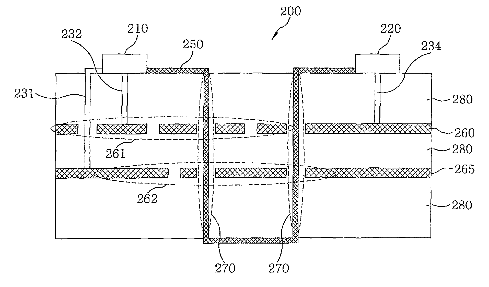
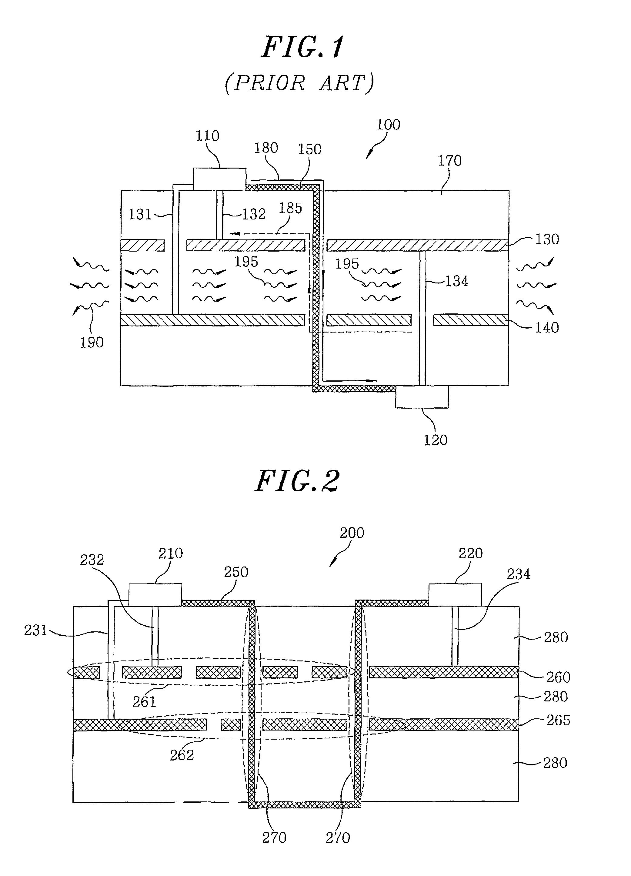
The present invention provides an electromagnetic-wave suppression structure for a multilayer PCB or package structure. This structure can effectively suppress noises and improve signal characteristics. The structure is placed near a noise source or a device sensitive to electromagnetic-wave. The structure can be formed on a power plane and / or a ground plane and can be different in size and form for different uses. The structure has a band rejection characteristic with respect to a surface current. The invention can be achieved by combining electromagnetic-wave suppression structures with different cut-off frequencies.

Problems solved by technology

As an operation speed of high speed digital system increases and a clock frequency is at several GHz, simultaneous switching noise (SSN) is generated in an on / off chip, a multi-layer printed circuit board (PCB) or a package structure and is problematic.
The SSN can cause the significant problems with signal / power integrity (SI / PI), as well as electromagnetic interference (EMI), exciting the cavity resonance modes within parallel plate waveguide-type power / ground planes.
And then the propagated noises may affect an adjacent signal lines or devices, finally causing the SI / PI problem.
However, a decoupling capacitor mounted in the multi-layer PCB may increase a production cost, make it difficult to dispose other devices in a limited space of the PCB, and cause another parallel resonance frequency due to its parasite inductance.
In addition, the decoupling capacitor has too low operation frequency of hundreds of MHz to effectively suppress the SSN in a GHz band that is problematic in high-speed systems.
However, such an EBG structure initially proposed as a mushroom shape of a two-layer structure has problems of complex process of forming a blind via and high production cost.

Method used


Image

  • Arrangement structure of electromagnetic band-gap for suppressing noise and improving signal integrity
  • Arrangement structure of electromagnetic band-gap for suppressing noise and improving signal integrity
  • Arrangement structure of electromagnetic band-gap for suppressing noise and improving signal integrity

Examples


Embodiment Construction

[0038]Hereinafter, the embodiments of the present invention will be described in detail with reference to the accompanying drawings.

[0039]Referring to FIG. 1, there is shown a current flow path, and SSN and EMI generation mechanism in a conventional multi-layer PCB or package structure 100 using a high speed signal. In the conventional multi-layer PCB or package structure 100, a driving circuit 110 is connected to the power plane 140 and the ground plane 130 through via 131 to be supplied with a power therethrough. A signal generally flows from the driving circuit 110 to a load 120 along a metal signal line 150. Here, in case of a high speed signal, a return current path 185 is not established through only the ground plane 130 but along a path having low input impedance in each layer when the signal is at a higher frequency. That is, when a high frequency signal and / or a high speed signal is used, both the ground plane 130 and the power plane 140 may be used as the return current pa...


PUM


Abstract

An electromagnetic-wave suppression structure in a multilayer PCB or package structure is supplied with a power to be used therein by a power distribution network including a power plane and a ground plane. The multilayer PCB and package includes: an electromagnetic-wave suppression structure including an electromagnetic band-gap; and the electromagnetic-wave suppression structure is formed at a specific portion(s) of the power plane and / or the ground plane to suppress noises.

Description

CROSS-REFERENCE(S) TO RELATED APPLICATION[0001]The present invention claims priority of Korean Patent Application No. 10-2008-0131836, filed on Dec. 22, 2008, which is incorporated herein by reference.FIELD OF THE INVENTION[0002]In general, an electric / electronic system using a high speed signal is applied with multilayer PCB (Printed Circuit Board) and package structure to provide various high technology functions. In order to stably supply a power and ground to devices and components in the PCB and package, the system has a power distribution network (PDN), formed of a pair of power plane and ground plane embedded within its multilayer structure. The present invention relates to a method for arranging an unwanted electromagnetic-wave suppression structure such as Electromagnetic Band-gap (EBG) for suppressing noises generating in a power distribution network used in the multilayer PCB and package. More particularly, the present invention relates to arrangement of electromagnetic-w...

Claims


Application Information

Patent Timeline
Patent Type & Authority Patents(United States)
IPC IPC(8): H04B3/32
CPCH05K1/0236H05K2201/09309H05K2201/09627H05K9/00H01L23/12H05K3/46
Inventor KWON, JONG HWASIM, DONG-UKKWAK, SANG ILYUN, JE HOONKIM, CHANG-JOO
Owner ELECTRONICS & TELECOMM RES INST
Learn More