Microelectrode, applications thereof and method of manufacturing

a microelectrode and microelectrode technology, applied in the field of microelectrodes, can solve the problems of reducing the battery life of the implantation, affecting the operation efficiency of the implantation device,

Inactive Publication Date: 2011-08-30
NANO BIOSENSORS
View PDF10 Cites 36 Cited by
  • Summary
  • Abstract
  • Description
  • Claims
  • Application Information

AI Technical Summary

Benefits of technology

According to still further features in the described preferred embodiments the metallic layer(s) is capable of preventing penetration of macromolecules therethrough.

Problems solved by technology

It is recognized that if the electrode is located as little as 2 mm away from the desired target, ineffective stimulation results due to several reasons: (i) failure to capture control of the group of neurons, (ii) stimulation of non-desirable areas resulting in unpleasant stimulation, or (iii) necessity for higher stimulus intensities to produce the desired effect resulting in reduced battery life of the implantation, or an any combination of these or other reasons.
The above systems, however, suffer from many limitations.
It is recognized that the replacement of the micro-electrode results in severe complication of the procedure because the replaced electrode never return to its original coordinate.
Moreover, stimulation of neighboring brain areas results in various complications, such as undesired side effects, include tingling sensation (paresthesia), worsening of symptoms, speech problems (dysarthria, dysphasia), dizziness or lightheadedness (disequilibrium), facial and limb muscle weakness or partial paralysis (paresis), involuntary muscle contractions (dystonia, dyskinesia), movement problems or reduced coordination, jolting or shocking sensation and numbness (hypoesthesia).
Although numerous attempts have been made to improve the procedure, e.g., by providing a macroelectrode with several leads, the improvement is still far from being satisfactory.
This is primarily due to the size of the macroelectrode which it too large for performing accurate specific stimulation.
The main reason for the lack of suitable electrode for accurate specific stimulation is the difficulty in the manufacturing process.
Unfortunately, the mechanical and electrical properties of the microelectrode are conflicting features because materials which posses good mechanical properties have less than optimal electrical properties and vice versa.
For example, tungsten can be used to manufacture a stiff microelectrode, but such microelectrode is known to undergo corrosion.
Moreover, the price of noble metals is expensive, especially iridium.
However, heretofore these metals-alloys were only used to manufacture thick substrates, because only thick substances posses sufficient mass and heat capacitance to tolerate the high temperature of the PVD process.

Method used


Image

  • Microelectrode, applications thereof and method of manufacturing
  • Microelectrode, applications thereof and method of manufacturing
  • Microelectrode, applications thereof and method of manufacturing

Examples


Embodiment Construction

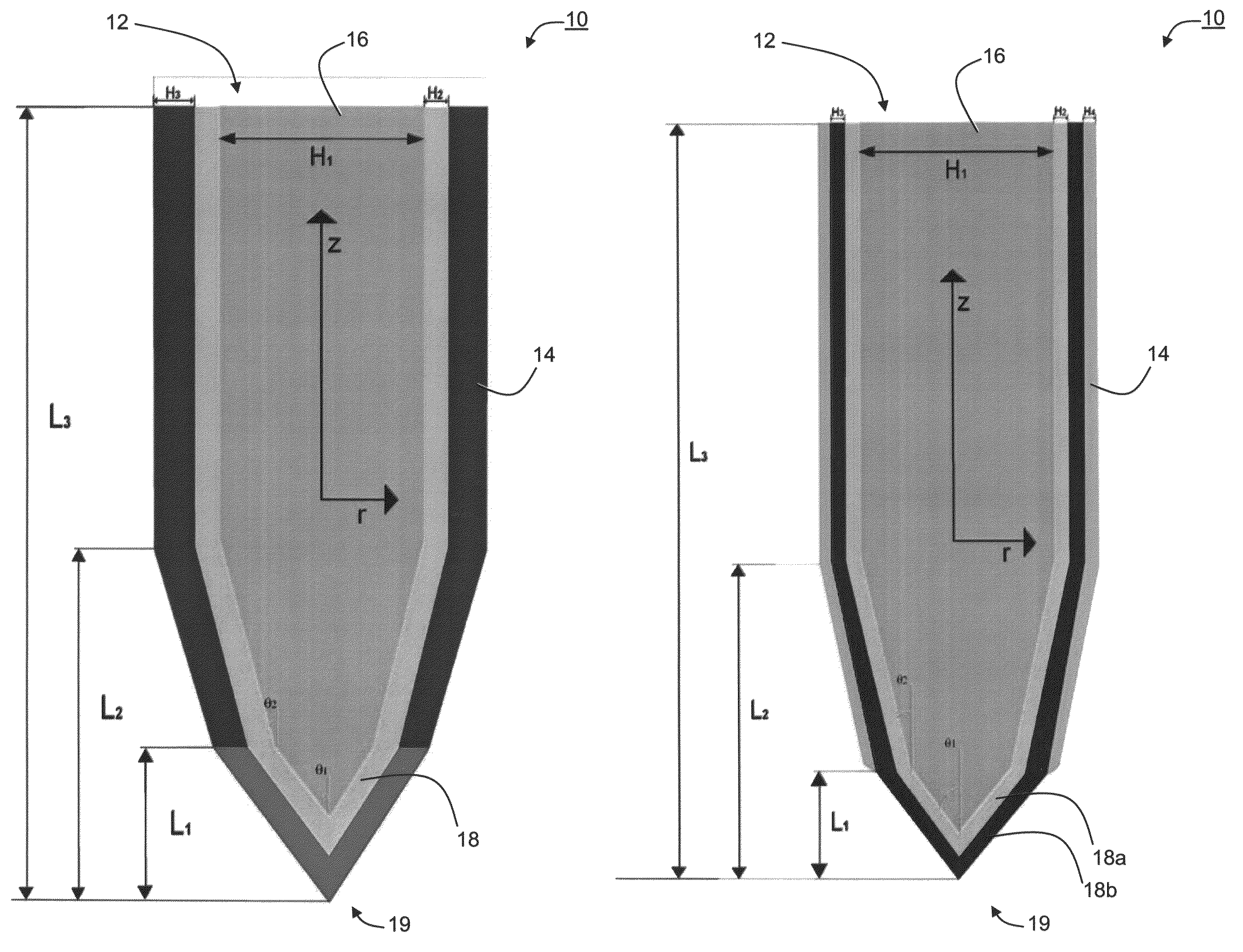
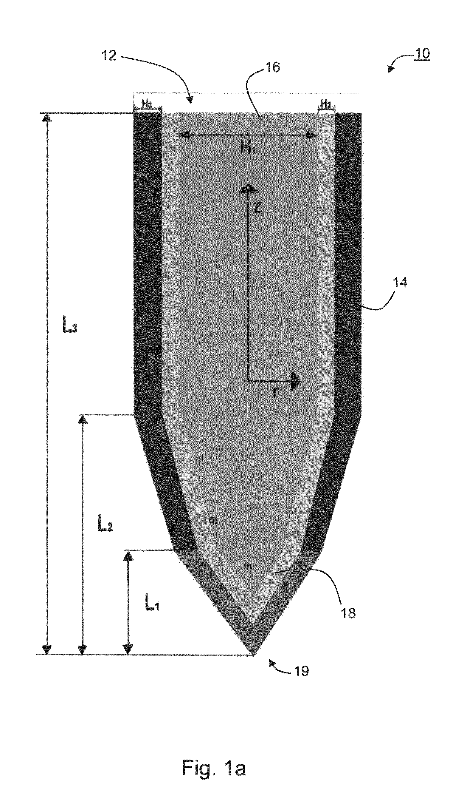
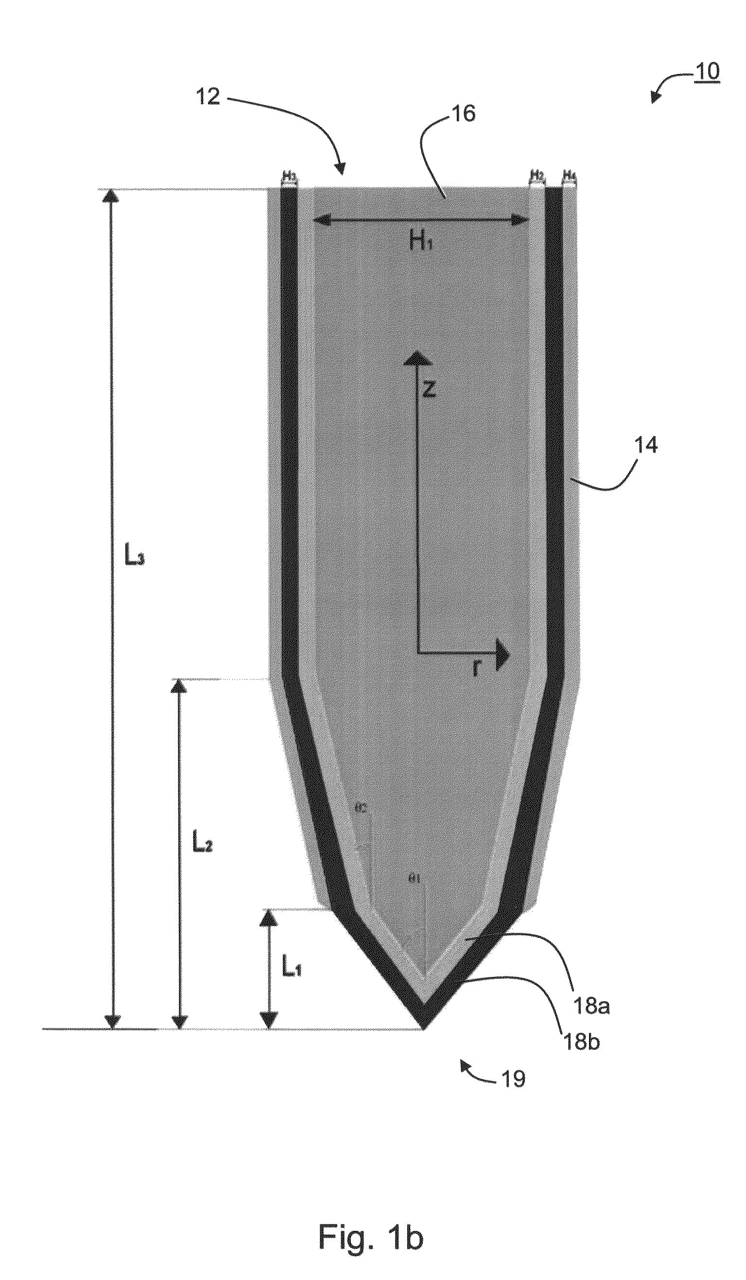
The present embodiments comprise a microelectrode device which can be used in various applications, including, without limitation, medical applications. Specifically, but not exclusively, the present embodiments can be used for deep brain stimulation, neuromonitoring, spinal stimulation, peripheral nerve stimulation, cardiac monitoring, cardiac rhythm management, ablation, mapping and the like. The present embodiments further comprise an electrode assembly, an implantable device and a system which incorporate the microelectrode device. Various exemplary embodiments of the invention comprise a method of manufacturing the electrode device and a method of implanting the implantable device.

The principles and operation of the method, system and device in accordance with preferred embodiments of the present invention may be better understood with reference to the drawings and accompanying descriptions.

Before explaining at least one embodiment of the invention in detail, it is to be unders...


PUM

PropertyMeasurementUnit
pore sizeaaaaaaaaaa
diameteraaaaaaaaaa
diameteraaaaaaaaaa

Abstract

An electrode device is disclosed. The electrode device comprises an electrically conductive core of micrometric size coated by at least one electrically isolating layer. The electrically conductive core comprises a substrate coated by at least one metallic layer having a nanometric pattern thereon and being at least partially exposed at a tip of the electrically conductive core.

Description

FIELD AND BACKGROUND OF THE INVENTIONThe present invention relates to microelectrodes and, more particularly, but not exclusively, to microelectrodes useful for medical purposes, such as, but not limited to, monitoring of electrical activity and stimulation of neurons, e.g., in the central nervous system.A wide variety of mental and physical processes are controlled or influenced by neural activity in particular regions of the brain. For example, various physical or cognitive functions are directed or affected by neural activity within the sensory or motor cortices. Across most individuals, particular areas of the brain appear to have distinct functions. In the majority of people, for example, the areas of the occipital lobes relate to vision; the regions of the left interior frontal lobes relate to language; portions of the cerebral cortex appear to be consistently involved with conscious awareness, memory, and intellect; and particular regions of the cerebral cortex as well as the...

Claims


Application Information

Patent Timeline
Patent Type & Authority Patents(United States)
IPC IPC(8): A61N1/05
CPCA61N1/05A61N1/0529A61N1/0551A61N1/3605
Inventor NIMER, EMADJADAON, NABILSILBAQ, FAUZI
Owner NANO BIOSENSORS
Why Eureka
Try Eureka