Growth of high quality low-loss ferrite materials on wide bandgap semiconductor substrates

a technology of ferrite materials and semiconductor substrates, which is applied in the direction of waveguide devices, magnetic bodies, transportation and packaging, etc., can solve the problems of limiting factors, inability to deposition ferrites on semiconductor substrates, and the need for integration of these ferrite devices with semiconductor platforms, so as to reduce strain, reduce microwave losses, and reduce chemical interdiffusion. effect of

Inactive Publication Date: 2011-10-04
THE UNITED STATES OF AMERICA AS REPRESENTED BY THE SECRETARY OF THE NAVY
View PDF3 Cites 0 Cited by
  • Summary
  • Abstract
  • Description
  • Claims
  • Application Information

AI Technical Summary

Benefits of technology

[0011]One aspect of the present invention is to gradually reduce the interfacial stress and mediate the strain between the plurality of layers in an embodiment of the present invention.
[0012]An additional aspect of the present invention is to allow for proper crystal alignment resulting in high crystal quality and thereby producing low microwave losses in an embodiment of the present invention.
[0015]A still further aspect of the present invention employs the buffer layer operable to minimize chemical interdiffusion between the ferrite layer and the wideband gap semiconductor material layer.
[0016]The above described disadvantages are overcome and advantages realized by the present invention including a device comprising a ferrite layer, a wideband gap semiconductor material layer, a buffering layer disposed between the ferrite layer and the wideband gap semiconductor material layer, wherein the buffering layer reduces strain at an interface between the ferrite layer and the wideband gap semiconductor material layer, and wherein the buffering layer produces a crystalline quality device for use in microwave frequency applications resulting in acceptably low microwave losses.

Problems solved by technology

In addition, one long standing problem facing the ferrite materials and device communities is the need for integration of these ferrite devices with semiconductor platforms (i.e. CMOS systems).
This has been the limiting factor.
The deposition of ferrites onto a semiconductor substrate is currently not possible due to the mismatch in lattice parameters between BaM and SiC, for example.
In other words, the atoms within the ferrite (BaM) layer and the semiconductor (SiC) layer are unable to properly align causing strains and poor crystal alignment.
In microwave applications, for example, this mismatch leads to unacceptable losses.
Furthermore, the atomic lattice mismatch between SiC and BaM is less than 5% allowing for their possible integration.

Method used


Image

  • Growth of high quality low-loss ferrite materials on wide bandgap semiconductor substrates
  • Growth of high quality low-loss ferrite materials on wide bandgap semiconductor substrates
  • Growth of high quality low-loss ferrite materials on wide bandgap semiconductor substrates

Examples


Embodiment Construction

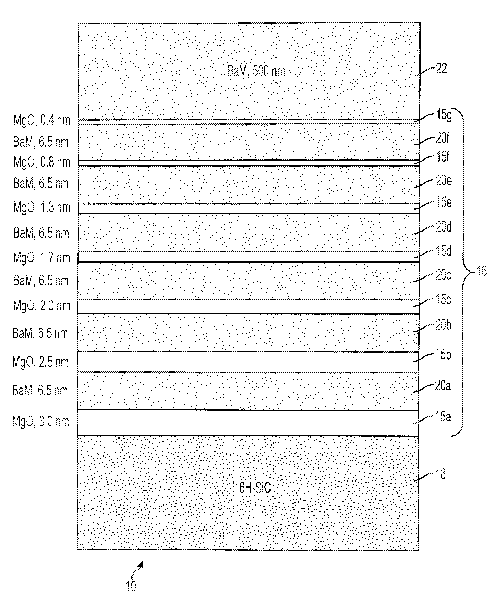
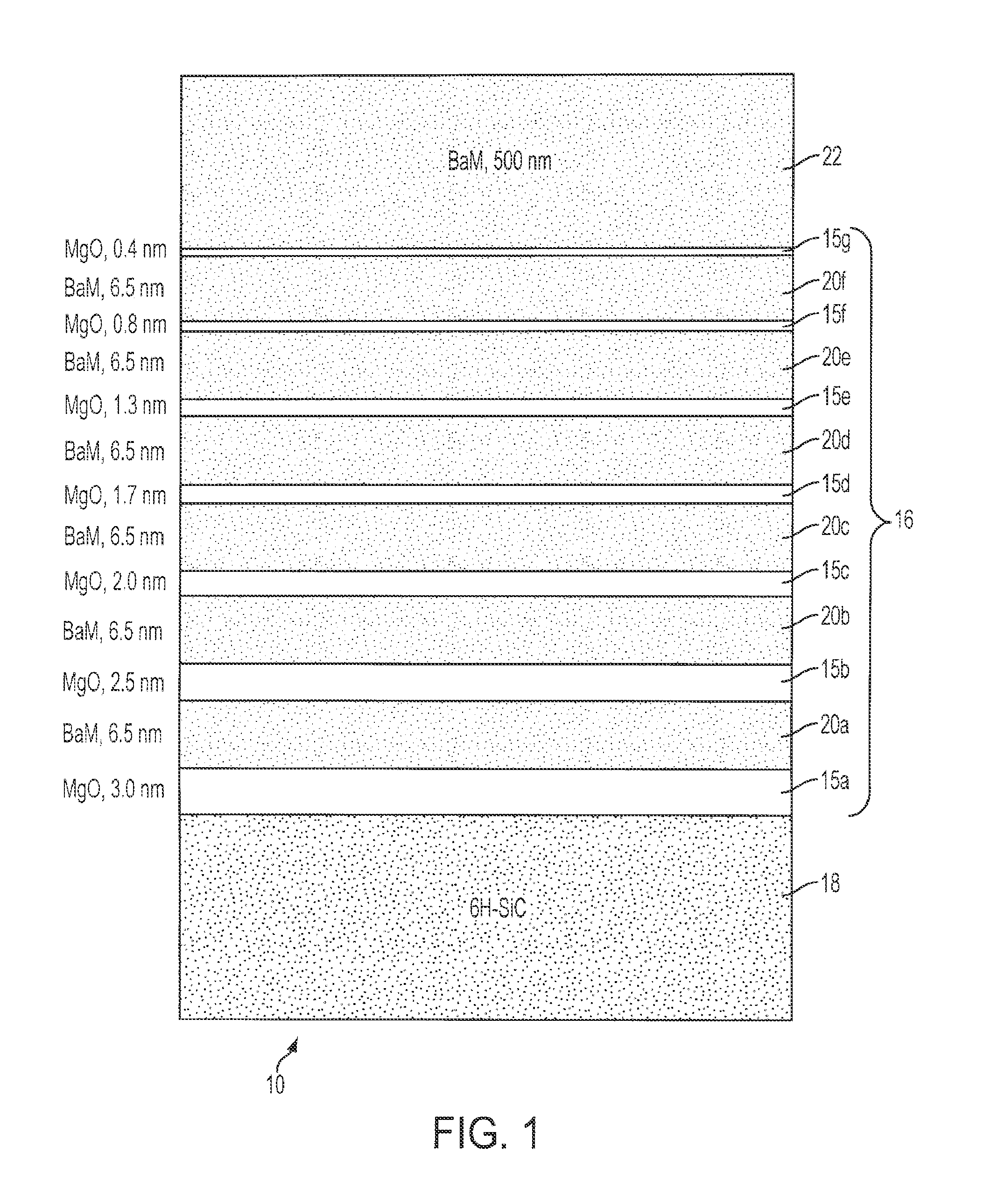
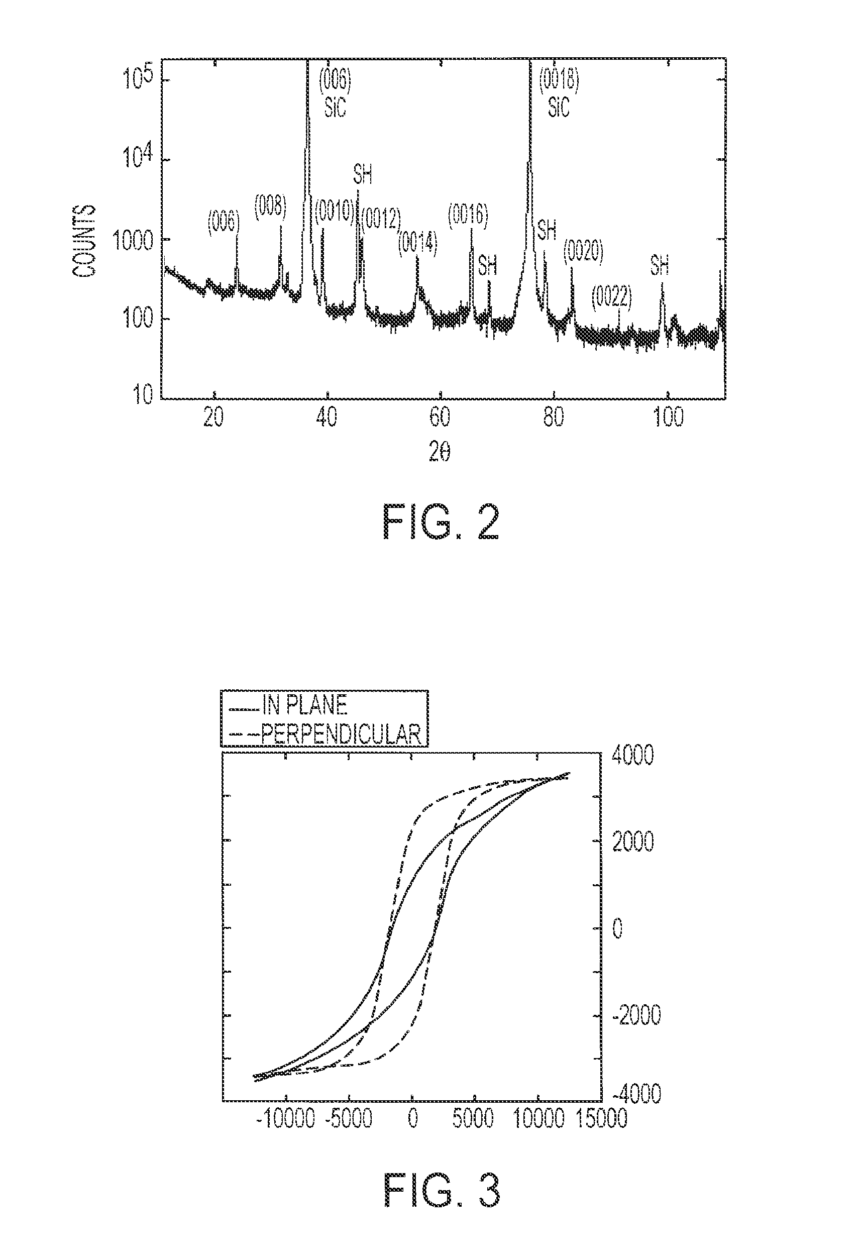
[0024]The present invention comprises a plurality of layers 10 including a hexaferrite layers 20a-f, a buffer layer 16 and a silicon carbide layer 18. The buffer layer 16 comprises a plurality of magnesium oxide (MgO) layers 15a-g and barium hexaferrite (BaM) layers 20a-f. The layers 15a-g and layers 20a-f can be interwoven to produce buffer layer 16, in an additional embodiment of the present invention. These layers act to gradually reduce the interfacial stress, mediate the strain and allow for proper crystal alignment resulting in high crystal quality and thereby producing low microwave losses in the applications in which the plurality of layers 10 are employed. High crystal quality results in low microwave losses as determined by low ferromagnetic resonance (FMR) linewidths. Moreover, the high crystal alignment needed in the microwave applications mentioned above, are achieved by an embodiment of the present invention and demonstrated by X-ray diffraction data as discussed in de...


PUM

PropertyMeasurementUnit
thicknessaaaaaaaaaa
thicknessaaaaaaaaaa
thicknessaaaaaaaaaa

Abstract

A semiconductor device including a ferrite layer, a widebandgap semiconductor material layer, and a buffer layer. The buffer layer comprises an interweaving of MgO and BaM. In addition the buffer layer allows a gradual reduction of the interfacial stress, and mediates the strain between a silicon substrate and a ferrite layer of the device. In addition, the buffer layer allows for high crystal alignment resulting in high crystal quality and thereby producing a low microwave loss semiconductor device. The buffer layer also minimizes chemical interdiffusion of atoms between the substrate and the ferrite layer.

Description

CROSS REFERENCE TO RELATED APPLICATION[0001]The present application claims benefit under 35 U.S.C. §119 (e) of a provisional application filed Oct. 5, 2005, entitled “GROWTH OF HIGH QUALITY LOW-LOSS FERRITE MATERIALS ON SiC SUBSTRATES FOR MICROWAVE AND MM APPLICATIONS”, Application No. 60 / 723,454.BACKGROUND OF THE INVENTION[0002]1. Field of the Invention[0003]The present invention relates generally to semiconductor materials. More specifically, the present invention relates to growth of ferrite materials on a semiconductor substrate.[0004]2. Description of the Related Art[0005]The next generation of radar electronics employs simultaneous transmit and receive (STAR) technology incorporating magnetic ceramics in multiport devices allowing simultaneous transmission of electromagnetic signals. The applications of this technology are within radar systems that enable continuous tracking of multiple targets. This technology is also applicable in the wireless communications market as well, ...

Claims


Application Information

Patent Timeline
Patent Type & Authority Patents(United States)
IPC IPC(8): B32B15/04
CPCH01F10/205H01L23/645Y10T428/325H01L2924/0002H01L2924/00
Inventor HARRIS, VINCENT GCHEN, ZHAOHUI
Owner THE UNITED STATES OF AMERICA AS REPRESENTED BY THE SECRETARY OF THE NAVY
Why Eureka
Try Eureka