

Field effect transistor for detecting ionic material and method of detecting ionic material using the same
a field effect transistor and ionic material technology, applied in the direction of material analysis, instruments, radio frequency controlled devices, etc., can solve the problems of difficult to reduce the overall size of the sensor, unstable voltage, etc., to improve the signal-to-noise ratio, improve scattering, and accurately detect ionic materials
- Summary
- Abstract
- Description
- Claims
- Application Information
AI Technical Summary
Benefits of technology
Problems solved by technology
Method used
Image

Examples
example 1
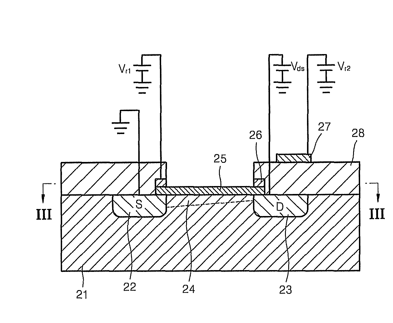
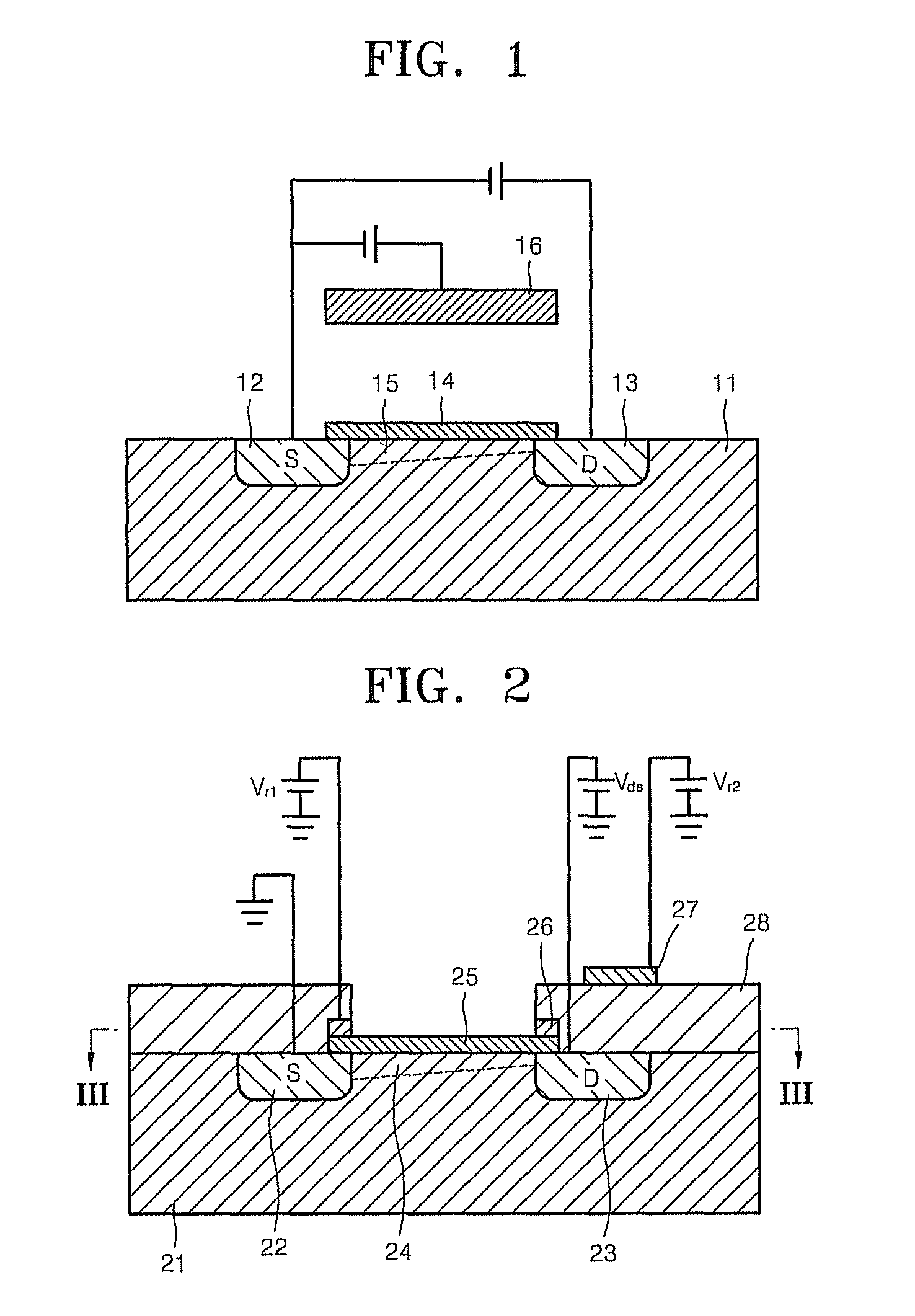
Manufacture of FET
A FET device used in the present invention was a conventional FET device manufactured by X-FAB Semiconductor Foundries (Germany). This device had 192 FETs, all having the same structure and arranged in an array shape (12×16). The FET device was manufactured using a complementary metal-oxide semi-conductor (“CMOS”) process and equipment, both owned by X-FAB Semiconductor Foundries. CMOS manufacturing processes slightly differ according to company, and thus, a detailed description thereof is omitted herein for brevity.
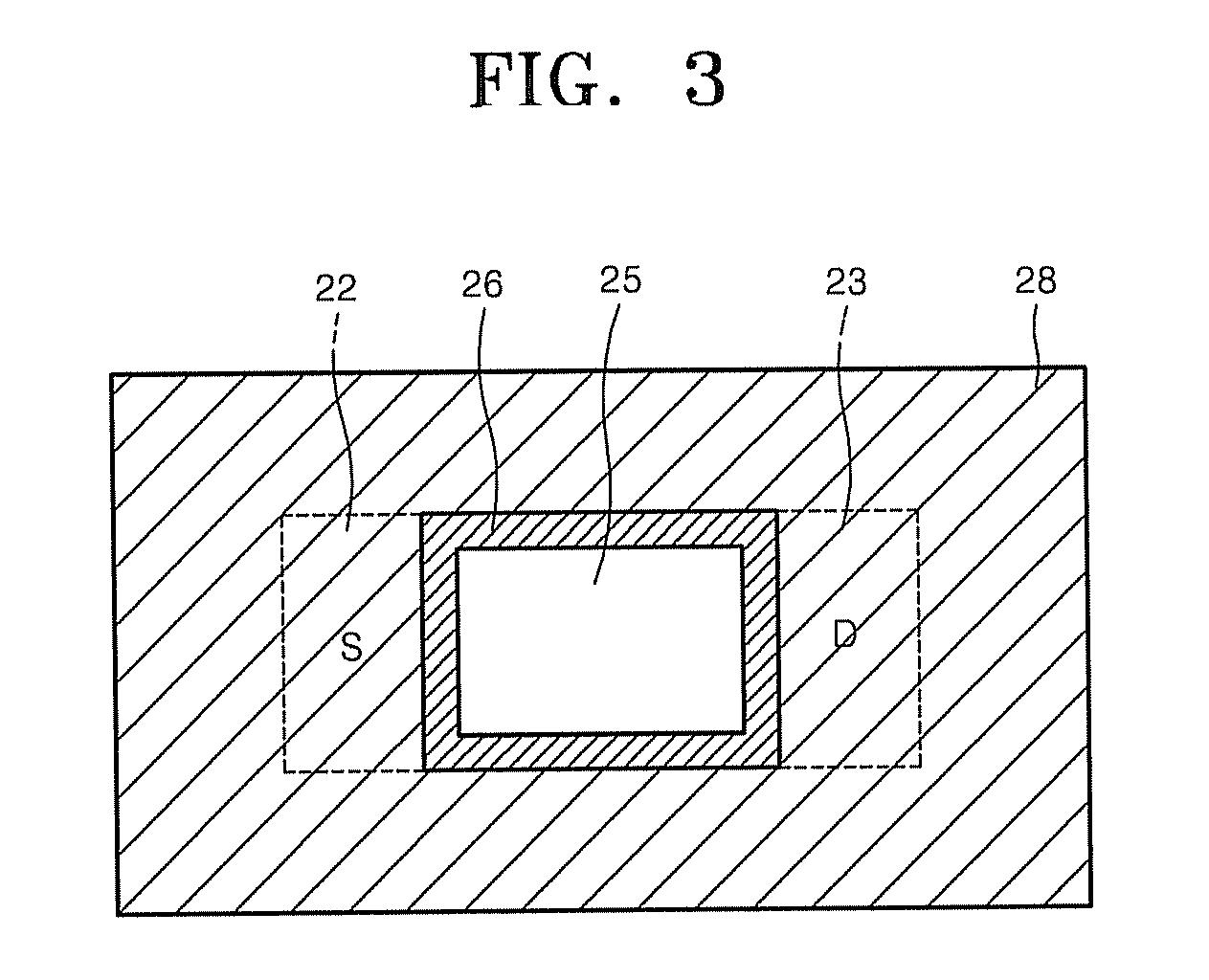
The upper surface of the FET device manufactured as described above was etched as illustrated in FIGS. 2 and 3. In other words, the passivation layer and the gate electrode layer of each FET were removed to expose a silicon oxide layer, that is, the insulating layer 25. As clearly illustrated in FIG. 3, instead of etching the entire gate electrode layer, the middle portion of the gate electrode layer was etched to leave the edge portion thereof as the f...
experimental example 1
Detecting Solution Using FET
The two chambers each including the FET device manufactured according to Example 1 constituted a sensing chamber and a reference chamber.
0.01 millimole (mM) of a phosphate buffer (“PB”) solution (pH 5.88) continuously flowed in and out of the reference chamber. 0.01 mM of a PB solution (pH 5.88) firstly flowed into the sensing chamber, as in the reference chamber, and then, solutions containing different ionic materials, for example, 0.1 mM of a NaOAc solution (pH 4.72) and 0.01 mM of PB solution (pH 6.08), alternately flowed in and out of the sensing chamber.
A constant voltage was continuously applied to the source and drain regions of the FET included in the reference chamber and the sensing chamber, while the first reference electrode and the external and internal second reference electrodes were on and off.
The source and drain current according to inflow of solutions containing different pHs and the on-off state of the first reference electrode and th...
experimental example 2
Detecting PCR Products Using FET
An experiment was performed to identify whether the FET manufactured according to Example 1 could detect PCR products.
In order to do so, a solution including PCR products, a washing solution, and a negative control (“NTC”) solution were alternately injected to a FET based sensor.
In order to obtain the PCR products, Staphylococcus aureus bacteria template was used to perform a PCR amplifying process. The base sequence of forward and reverse primer used in the process was 5′-(TAG CAT ATC AGA AGG CAC ACC C)-3′ (SEQ ID NO: 1) and 5′-(ATC CAC TCA AGA GAG ACA ACA TT)-3′ (SEQ ID NO: 2), respectively. The PCR products obtained after the PCR amplifying process had the size of 240 base pairs (bp). In addition, the concentration of PCR products was diluted to be 5 nanograms per microliter (ng / μl) using phosphate buffer. The pH of the phosphate buffer containing PCR products was 5.49.
0.01 mM of phosphate buffer (pH 6.02) was used as the washing solution.
The NTC s...
PUM
 Abstract
Description
Claims
Application Information