Semiconductor memory device and method of forming the same

a memory device and semiconductor technology, applied in semiconductor devices, digital storage, instruments, etc., can solve the problems of dram read operation destructive, difficult to scale the area of capacitors, and the process of building capacitors adds to dram manufacturing complexity

Active Publication Date: 2012-01-03
SUZHOU ORIENTAL SEMICONDUCTOR CO LTD
View PDF8 Cites 13 Cited by
  • Summary
  • Abstract
  • Description
  • Claims
  • Application Information

AI Technical Summary

Benefits of technology

[0004]An example 6-transistor (6T) SRAM is shown in FIG. 5c. The cross-coupled inverters are used to store logic state “1” or “0”. Two access NMOS-FETs are used to access the storage nodes. The read operation of SRAM cell is non-destructive. Furthermore, SRAM can have very short time for write and read, e.g. 0.5 nano-second. For these reasons, SRAM is applied in Central Processing Unit (CPU) as L1 and L2 caches. The conventional SRAM cell is formed by 6 transistors, thus it has larger unit cell size compared to DRAM cell which usually has 1 access transistor and 1 capacitor (1T-1C). With the scaling of SRAM, the standby leakage current increases, resulting in an increasing power consumption. In addition, as the circuit scaled, the static noise margin window of 6-T SRAM gets smaller and the stability gets worse. In order to improve the static noise margin and stability, an 8-transistor SRAM cell was proposed by L. Chang, et al. [U.S. patent application: U.S. Pat. No. 7,106,620, B2]. The trade-off of improved stability is increased transistor numbers and therefore larger unit memory cell size.

Problems solved by technology

DRAM read operation is destructive and a write-back sequence is needed to restore the read bits.
In addition, the capacitance of the storage capacitor must not be too low in order to store sufficient charge.
Thus, the area of capacitor is difficult to be scaled and the processes for building capacitor add to DRAM manufacturing complexity.
Furthermore, SRAM can have very short time for write and read, e.g. 0.5 nano-second.
With the scaling of SRAM, the standby leakage current increases, resulting in an increasing power consumption.
In addition, as the circuit scaled, the static noise margin window of 6-T SRAM gets smaller and the stability gets worse.
However, FBC usually requires SOI substrate which is usually more expensive than the conventional bulk silicon substrate.
In addition, only very limited number of charges are stored in the floating body, as results in poor retention performance.
Further, the performance of FBC is quite sensitive to temperature.
However, the junction leakage current in FBC is hard to be scaled when scaling down the FBC cell, the retention performance of FBC is usually much worse than 1T-1C DRAM even with back-gate bias[4].
FBC has the smallest unit cell size and simplest structure but the data retention performance is poor.

Method used


Image

  • Semiconductor memory device and method of forming the same
  • Semiconductor memory device and method of forming the same
  • Semiconductor memory device and method of forming the same

Examples


Embodiment Construction

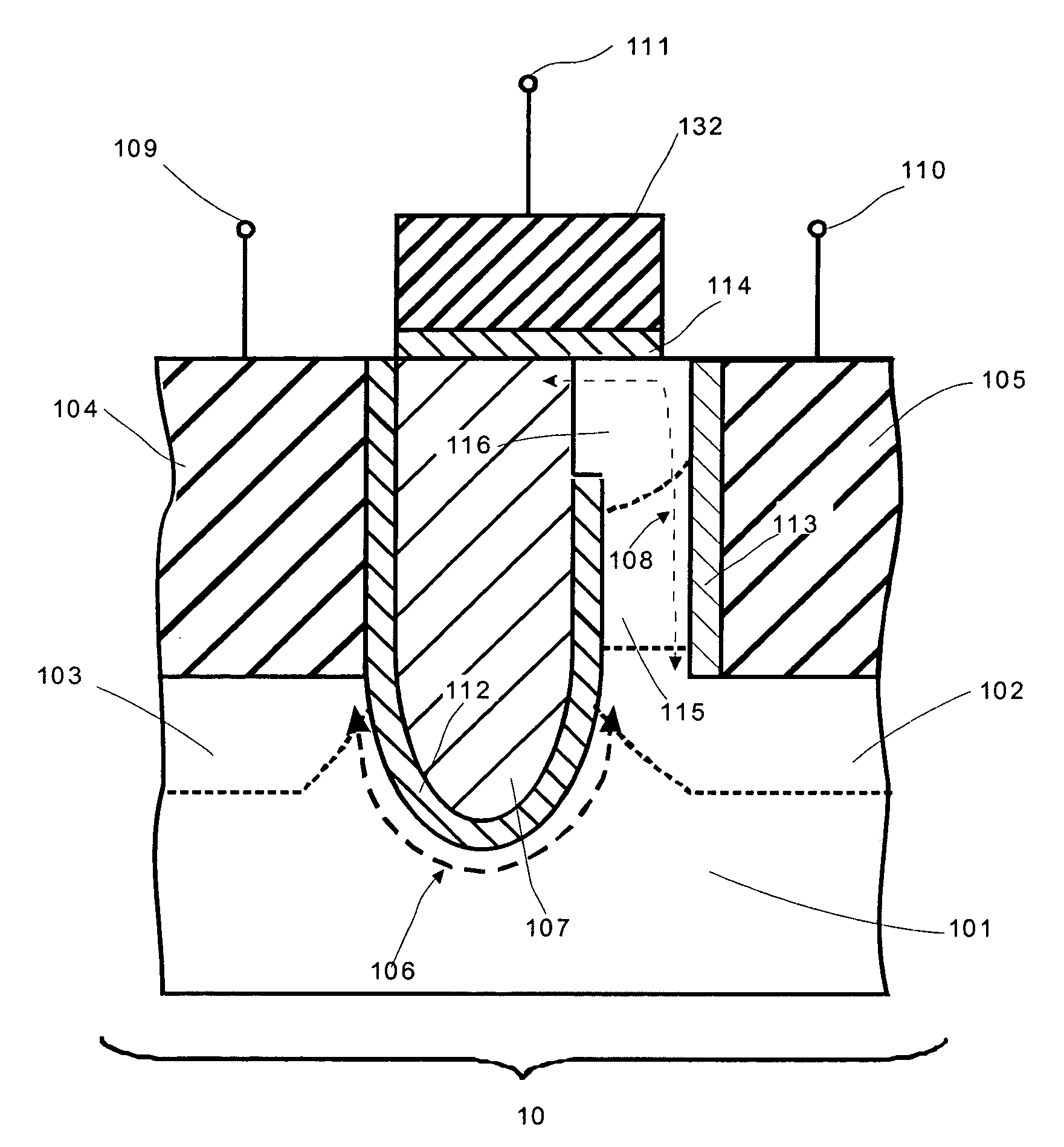
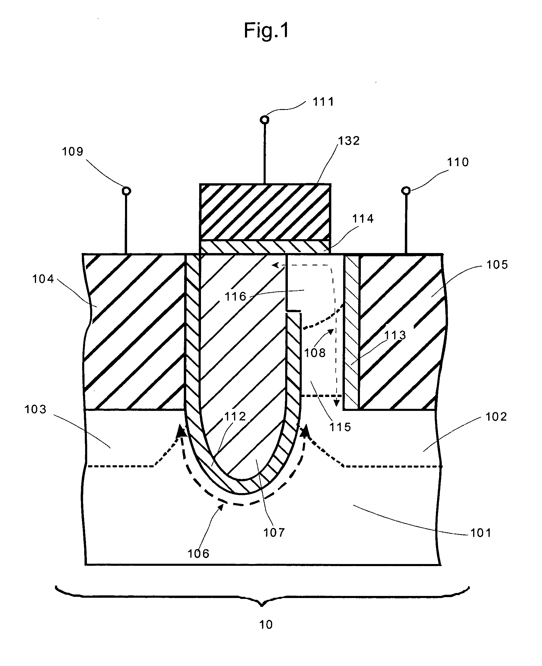
[0018]FIG. 1 illustrates an example cross-sectional view of the disclosed semiconductor memory cell 10 called floating junction gate (FJG) memory device. The FJG memory device 10 is usually formed in a semiconductor substrate or doped well 101 which has a light n-type or p-type doping concentration, e.g. doping level lower than 2×1018 cm−3. The substrate material can be single crystal silicon or silicon on insulator. Source 103, drain 102 are usually anti-doped to well or substrate 101. The channel region 106 is between the source 103 and the drain 102. It is recessed into substrate 101 in order to increase the length of the channel. Region 103 acts as source of a MOSFET and it can be connected to an external electrode 109 directly or via a source contact plug 104. Region 102 acts as drain of a MOSFET and can be connected to an external electrode 110 directly or via a drain contact plug 105. When the FJG device is turned on, current can flow between the drain 102 and the source 103 ...


PUM


Abstract

The present invention discloses a semiconductor memory device comprising a source, a drain, a floating gate, a control gate, a recess channel and a gated p-n diode. The said p-n diode connects said floating gate and said drain. The said floating gate is for charge storage purpose, it can be electrically charged or discharged by current flowing through the gated p-n diode. An array of memory cells formed by the disclosed semiconductor memory device is proposed. Furthermore, an operating method and a method for producing the disclosed semiconductor memory device and array are described.

Description

BACKGROUND OF THE INVENTION[0001]Semiconductor memory devices are widely used in many electronic products. Depending on the field of application, memory cell types having different operating speed and density are desired. For example, static random access memory (SRAM) is optimized for high random access speed, while stand alone dynamic random access memory (DRAM) is optimized for high density but moderate random access speed.[0002]FIG. 5a-c illustrate semiconductor memory cells of prior arts. 1T-1C DRAM cell is shown in FIG. 5a; floating body cell (1T-DRAM) is shown in FIG. 5b; 6T-SRAM cell is shown in FIG. 5c. [0003]A conventional 1T-1C DRAM cell 500 consists of 1 access transistor 503 and 1 capacitor 504. When operating a 1T-1C DRAM cell, a logic bit can be assigned to a cell, wherein a first logic state of the bit can be assigned to the state with high potential and a second logic state of the bit can be assigned to the memory cell with lower potential. When reading a 1T-1C memo...

Claims


Application Information

Patent Timeline
Patent Type & Authority Patents(United States)
IPC IPC(8): G11C11/24
CPCG11C11/404H01L21/28273H01L29/42336H01L29/66825H01L29/788G11C2211/4016H01L2924/0002H01L2924/00H01L29/40114
Inventor WANG, PENG-FEIGONG, YI
Owner SUZHOU ORIENTAL SEMICONDUCTOR CO LTD
Why Eureka
Try Eureka