Method and structure to control thermal gradients in semiconductor wafers during rapid thermal processing

a technology of thermal processing and semiconductor wafers, applied in the field of system and method for controlling thermal gradients in silicon wafers during thermal processing, can solve the problems of inability to maintain uniform temperature distribution, inability to accept wafer damage, and catastrophic breaking of wafers

Inactive Publication Date: 2012-01-31
ALSEPHINA INNOVATIONS INC
View PDF11 Cites 8 Cited by
  • Summary
  • Abstract
  • Description
  • Claims
  • Application Information

AI Technical Summary

Benefits of technology

[0015]A method of thermally processing a workpiece is provided in accordance with another aspect of the invention. In such method, the workpiece is supported within a chamber by at least three upwardly extending elongated support members. Each of the support members includes a first portion adjacent to the workpiece. The first portion can have a first thermal response which is faster than a thermal response of the workpiece. A second portion extends downwardly from the first portion. The second portion can have a second thermal response which is slower than or equal to the thermal response of the workpiece. Heat is transferred to or from the workpiece. When a temperature of the first portion of each support member changes at least as rapidly as the workpiece, there is no net flow of heat from the workpiece into the support members.

Problems solved by technology

However, faster heating ramp rates increase the difficulties to maintain uniform temperature distribution over the functional wafer surface at the desired peak processing temperature of interest.
In many tools, fused silica is the material of choice for the fabrication of these support pins because this material has both low thermal conductivity and low thermal expansion coefficient.
Lateral displacements of contact points in the back side of the wafer can create micron size cracks on the wafer bottom surface which can later grow with further thermal treatments and precipitate unacceptable wafer damage and even catastrophic breaking of wafers.
But with the development of new processes with short peak temperature soaks usually shorter than a few seconds, fast ramp rates typically around −25-300° C. / second, and continuously shrinking complex structures to create new and more powerful transistor devices, the existing thermal processing window of 10° C. with a peak processing temperature, well above 1000° C., is not sufficient to generate wafers with acceptable yields.
The data thus collected shows that the wafer peak temperature distribution is lower on the regions of the wafer that surround the point where the support pins contact the wafer and do not meet the new requirements to be within a 2° C. thermal window.
Since the thermal conductivity of fused silica is the lowest relative to the conductivity of other materials also used in these types of applications, like silicon, silicon carbide or quartz itself, it is understandable that no thermal solutions are possible to minimize the local thermal gradient created by the existing tooling.

Method used


Image

  • Method and structure to control thermal gradients in semiconductor wafers during rapid thermal processing
  • Method and structure to control thermal gradients in semiconductor wafers during rapid thermal processing
  • Method and structure to control thermal gradients in semiconductor wafers during rapid thermal processing

Examples


examples

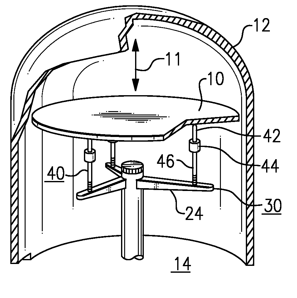
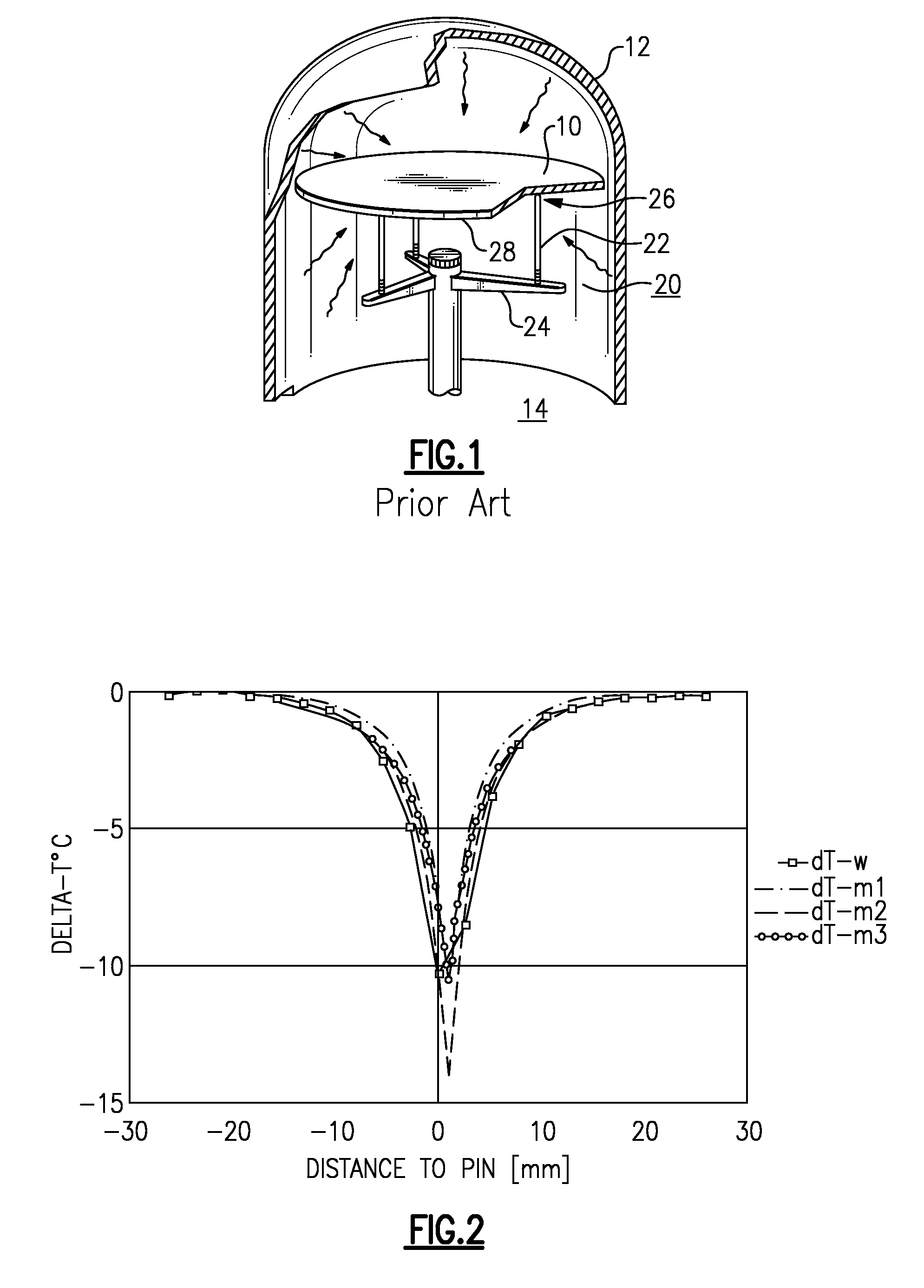
[0035]Examples shown in this section are predominantly obtained from model results. They show the agreement between the model prediction and the expectation flowing from the theory presented and description of the invention. However, actual wafer data is included in FIG. 2 for the purpose of validating the accuracy of the model and also calibrating the model against the unknown initial pin temperature.

[0036]In Table 1 and FIG. 2 is shown the effect of initial pin temperature. This parameter will effect the local temperature distribution in the wafer as the wafer is supported by the pin and heated. However, this parameter is also difficult to measure directly. By comparing model expectation as a function of initial pin temperature against actual wafer data, it is possible to obtain an engineering estimate of the initial pin temperature by selecting the condition which most closely matches actual experience. This is done in FIG. 2. It can also been seen from FIG. 2 that the relative b...


PUM


Abstract

An article supports a workpiece during thermal processing. At least three elongated support members, e.g., support pins, extend upwardly from an element such as support arms for supporting the workpiece. Each of the support members includes a first portion adjacent to the workpiece. A second portion extends downwardly from the first portion. The first portion can have a thermal response faster than the thermal response of the workpiece and the second portion can have a slower thermal response. A removable element may be mounted to the support member for adjusting the thermal response of the support member. With removable elements, the support members can be adjusted to cause no net transfer of heat to or from the workpiece.

Description

BACKGROUND OF THE INVENTION[0001]1. Field of the Invention[0002]The embodiments of the invention generally relate to a system and method for controlling thermal gradients in a silicon wafer during thermal processing.[0003]2. Description of the Related Art[0004]While the use of high temperature ovens for thermal processing of wafers to manufacture advanced integrated circuit chips have been in use for the past few decades or so, the use of rapid thermal processing and the requirement to control the wafer temperature gradients at the process peak temperature within a continuously decreasing processing window is a more recent development, mostly driven by the continuous reduction in the dimensions of the electronic transistors being fabricated in the wafer surface. Economic forces drive both the need to increase function integration within each silicon die and the need to develop new technologies to increase the processing capability of each die in a continuous effort to reduce the die...

Claims


Application Information

Patent Timeline
Patent Type & Authority Patents(United States)
IPC IPC(8): F26B19/00
CPCH01L21/67103H01L21/6875
Inventor BEZAMA, RASCHID J.GOLDMANN, LEWIS S.WALL, DONALD R.
Owner ALSEPHINA INNOVATIONS INC
Why Eureka
Try Eureka