Method of fabricating array substrate

a technology of array substrate and substrate layer, applied in the field of array substrate, can solve the problems of reducing the mobility of the active layer of intrinsic amorphous silicon, limiting the use of driving elements, and reducing the use of switching elements or driving elements, so as to reduce production costs and improve production yield

Active Publication Date: 2012-04-17
LG DISPLAY CO LTD
View PDF4 Cites 4 Cited by
  • Summary
  • Abstract
  • Description
  • Claims
  • Application Information

AI Technical Summary

Benefits of technology

[0017]An object of the present invention is to provide a method of fabricating an array substrate including a thin film transistor having improved properties.
[0018]Another object of the present invention is to reduce production costs and improve production yield for an array substrate.

Problems solved by technology

Accordingly, there is an disadvantage in a use for a switching element or a driving element.
In addition, the active layer of intrinsic amorphous silicon has a relatively low carrier mobility, for example, 0.1 to 1.0 cm2 / V·s, there is further limitation in a use for a driving element.
Accordingly, production costs are increased.
In addition, since the TFT in FIG. 2 has more complicated structure, production yield is reduced.

Method used


Image

  • Method of fabricating array substrate
  • Method of fabricating array substrate
  • Method of fabricating array substrate

Examples


first embodiment

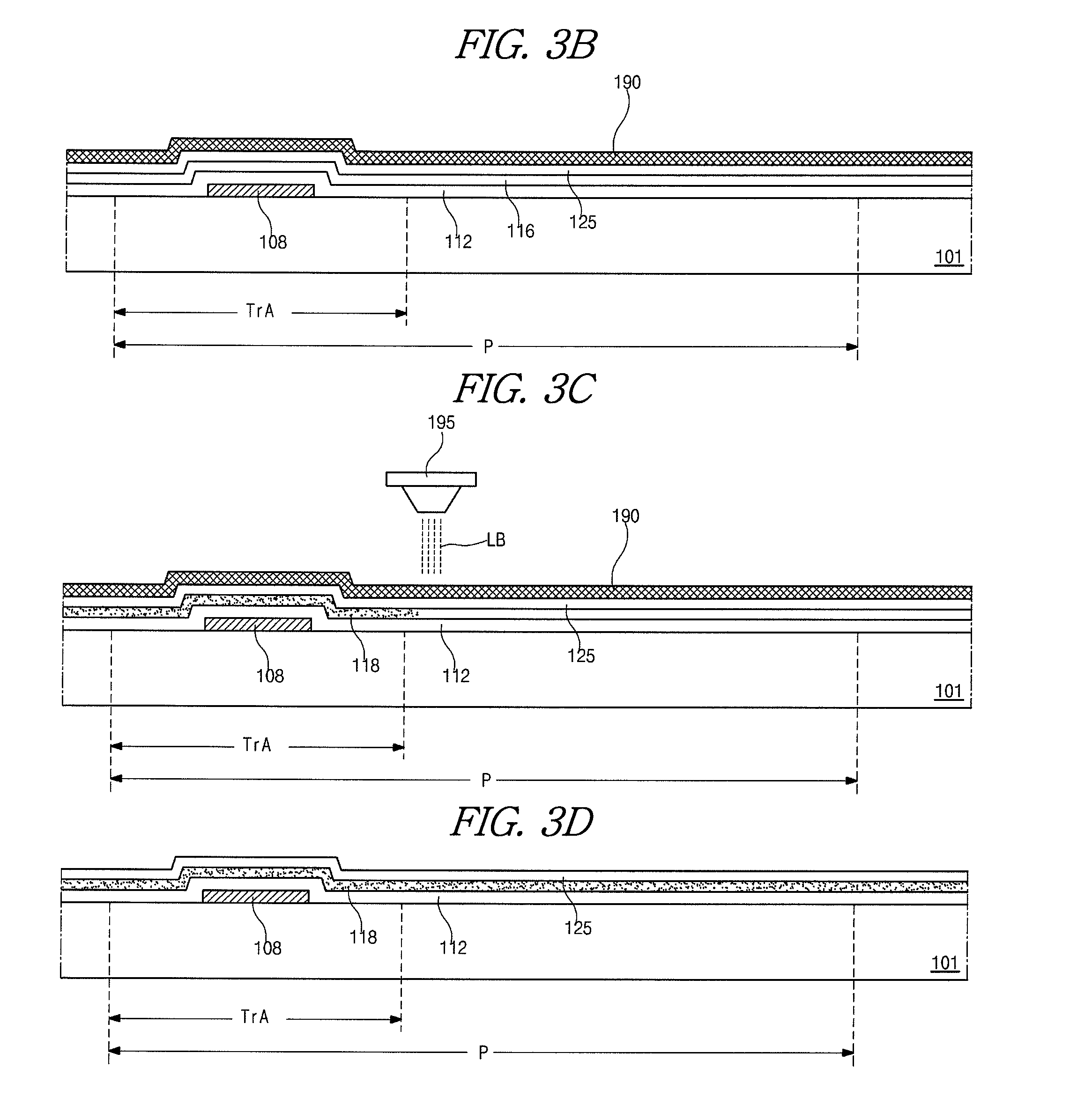
[0028]FIG. 3A to 3M are cross-sectional views of a fabricating process of an array substrate according to the present invention. For convenience of explanation, a switching region is defined in a pixel region.

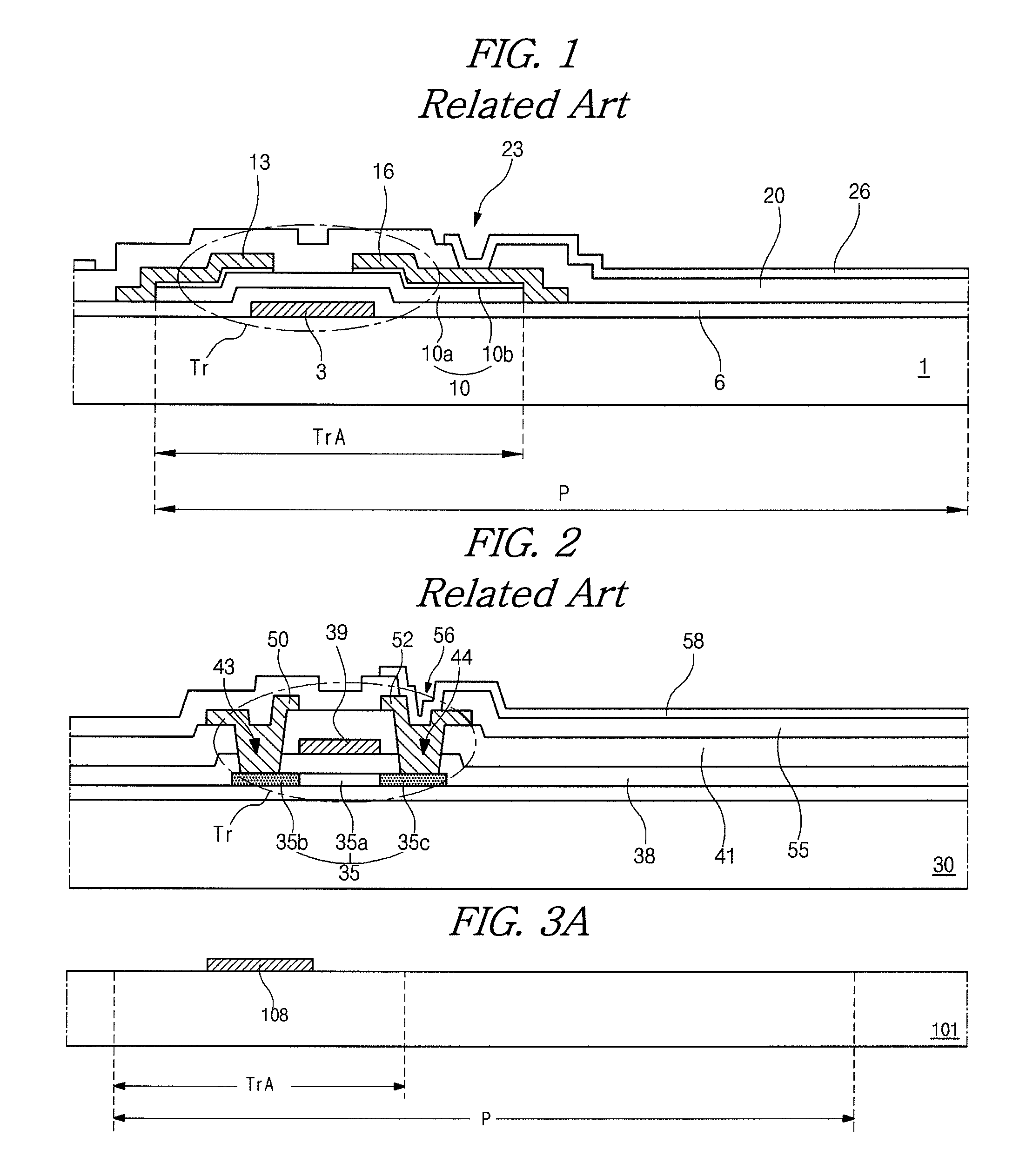
[0029]As shown in FIG. 3A, a first metal layer (not shown) is formed on a substrate 101 by depositing a first metallic material. For example, the first metallic material may include one of aluminum (Al), Al alloy (AlNd), copper (Cu), Cu alloy and chromium (Cr). The first metal layer is patterned by a first mask process to form a gate line (not shown) and a gate electrode 108 connected to the gate line. The mask process includes a step of forming a photoresist (PR) layer on the first metal layer, a step of exposing the PR layer using an exposing mask, a step of developing the exposed PR layer to form a PR pattern, a step of etching the first metal layer using the PR pattern as an etching mask and a step of stripping the PR pattern.

[0030]FIG. 3A shows the first metal layer having...

second embodiment

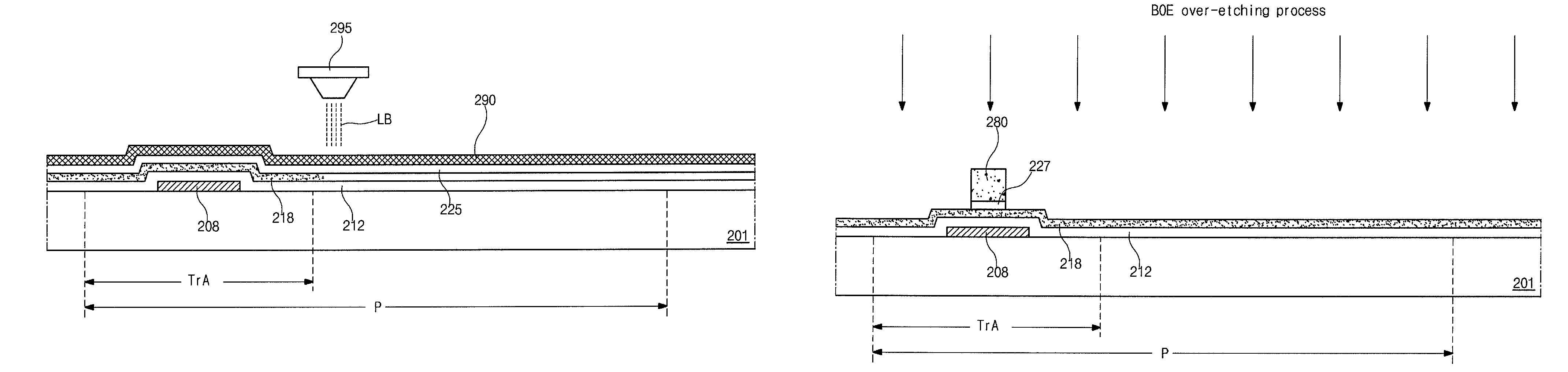
[0066]Next, as shown in FIG. 4L, a transparent conductive material layer (not shown) is formed on the passivation layer 240 by depositing a transparent conductive material. For example, the transparent conductive material may include indium-tin-oxide (ITO) or indium-zinc-oxide (IZO). The transparent conductive material layer is patterned by a fifth mask process to form a pixel electrode 250 in the pixel region P. The pixel electrode 250 is disposed on the passivation layer 240 and is connected to the drain electrode 238 through the drain contact hole 242. By the above process, the array substrate according to the present invention is obtained.

[0067]In the second embodiment, the array substrate is fabricated by a five mask process. Accordingly, there is advantages in production costs and production yield with compared to the first embodiment. In addition, since the gate insulating layer 212 is covered with the polycrystalline silicon layer 218 during the BOE over-etching process for ...


PUM

PropertyMeasurementUnit
carrier mobilityaaaaaaaaaa
wavelengthaaaaaaaaaa
energyaaaaaaaaaa

Abstract

A method of fabricating an array substrate includes forming a gate line and a gate electrode; forming a gate insulating layer, an intrinsic amorphous silicon layer, an inorganic material insulating layer and a heat transfer layer on the gate line and the gate electrode; irradiating a laser beam onto the heat transfer layer to crystallize the intrinsic amorphous silicon layer into a polycrystalline silicon layer; removing the heat transfer layer; patterning the inorganic insulating material layer using a buffered oxide etchant to form an etch-stopper corresponding to the gate electrode forming an impurity-doped amorphous silicon layer and a metal layer on the etch-stopper and the polycrystalline silicon layer; patterning the metal layer to form a data line, a source electrode and a drain electrode and forming a pixel electrode on the passivation layer.

Description

[0001]The present application claims the benefit of Korean Patent Application No. 10-2009-0112565, filed in Korea on Nov. 20, 2009, which is hereby incorporated by reference.BACKGROUND OF THE INVENTION[0002]1. Field of the Invention[0003]The present invention relates to an array substrate, and more particularly, to a method of fabricating an array substrate that includes a thin film transistor having excellent properties.[0004]2. Discussion of the Related Art[0005]As the society has entered in earnest upon an information age, a field of display devices that represent all sorts of electrical signals as visual images has developed rapidly. Particularly, the liquid crystal display (LCD) device or the OELD device as a flat panel display device having characteristics of light weight, thinness and low power consumption is developed to be used as a substitute for a display device of cathode-ray tube type.[0006]Since the LCD device including a thin film transistor (TFT) as a switching eleme...

Claims


Application Information

Patent Timeline
Patent Type & Authority Patents(United States)
IPC IPC(8): H01L21/84
CPCH01L21/268H01L27/1285H01L27/1248H01L27/1214H01L27/1274
Inventor LEE, HONG-KOOKIM, SUNG-KIBAE, JUN-HYEONKIM, KI-TAE
Owner LG DISPLAY CO LTD
Why Eureka
Try Eureka