Structures for controlling light interaction with microfluidic devices

a microfluidic device and light interaction technology, applied in fluorescence/phosphorescence, laboratory glassware, instruments, etc., can solve the problems of time-consuming alignment procedures, difficult to carry out accurate optical measurements (e.g., absorbance or transmission), and inability to accurately measure the absorbance or transmission of microchannels

Active Publication Date: 2012-07-17
OPKO DIAGNOSTICS
View PDF147 Cites 56 Cited by
  • Summary
  • Abstract
  • Description
  • Claims
  • Application Information

AI Technical Summary

Problems solved by technology

While various microfluidic methods and devices, such as microfluidic assays, can provide inexpensive, sensitive and accurate analytical platforms, carrying out accurate optical measurements (e.g., absorbance or transmission) on a microfluidic system can be challenging.
Optical measurements of microchannels may require, for example, time-consuming alignment procedures.
In addition, optical noise produced by light incident upon areas outside the channels may degrade the quality of the detected signal through the channels.

Method used


Image

  • Structures for controlling light interaction with microfluidic devices
  • Structures for controlling light interaction with microfluidic devices
  • Structures for controlling light interaction with microfluidic devices

Examples


example 1

Fabrication of Microfluidic Channels

[0127]A method for fabricating a microfluidic channel system is described.

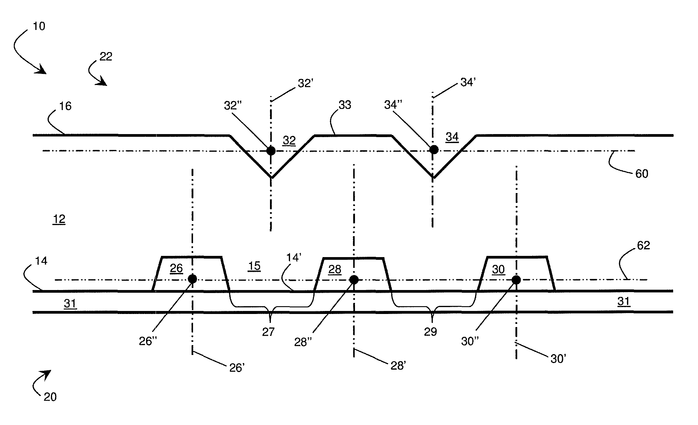
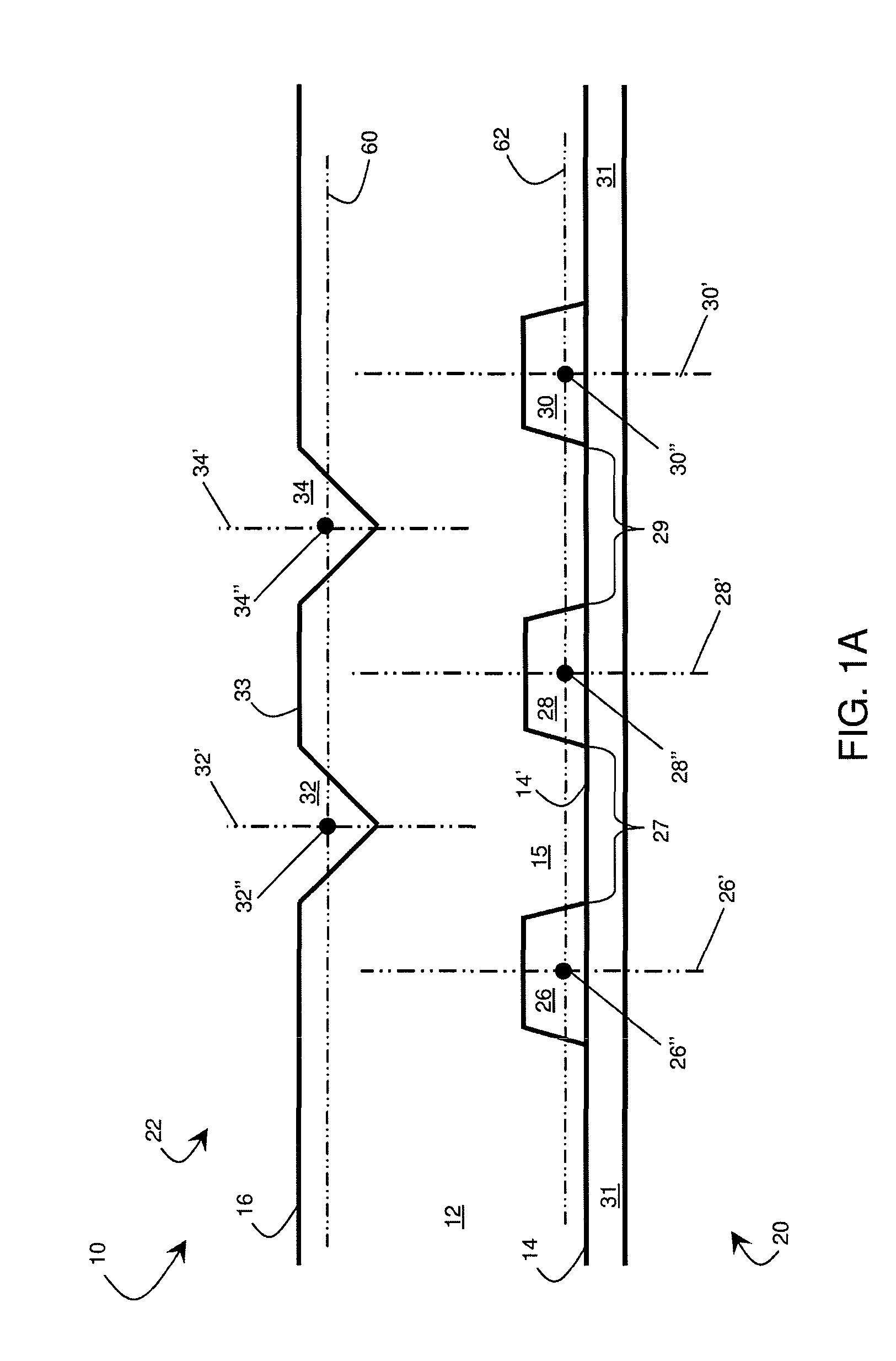
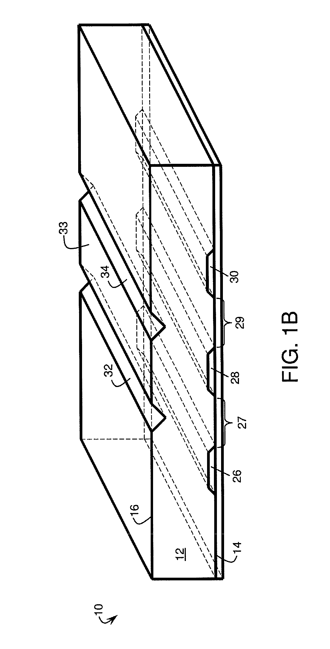
[0128]Channel systems, such as the ones shown in FIGS. 1A and 1B, were designed with a computer-aided design (CAD) program. The microfluidic devices were formed in poly(dimethylsiloxane) Sylgard 184 (PDMS, Dow Corning, Ellsworth, Germantown, Wis.) by rapid prototyping using masters made in SU8 photoresist (MicroChem, Newton, Mass.). The masters were produced on a silicon wafer and were used to replicate the negative pattern in PDMS. The masters contained two levels of SU8, one level with a thickness (height) of ˜70 μm defining the channels in the immunoassay area, and a second thickness (height) of ˜360 μm defining the reagent storage and waste areas. Another master was designed with channel having a thickness (height) of 33 μm. The masters were silanized with (tridecafluoro-1,1,2,2-tetrahydrooctyl)trichlorosilane (ABC-R, Germany). PDMS was mixed according to the manufacture...

example 2

Performance of a System Comprising Triangular Optical Elements

[0130]This example describes the transmission profiles of systems employing a meandering channel, one with triangular optical elements (grooves) and another without. An article was fabricated in polystyrene with identical systems of fluidic channels on one side. Some of these channels included triangular optical elements between the channels on the other side (shielded channels). Other channels did not include triangular optical elements between them (normal / standard channels with no shielding). The channels were 160 microns in width. Intervening portions between the channels were 60 microns in width. The article thickness was designed using the model described above. Triangular optical elements were also designed as described in the model above with an angle of 35.3°, a width of 160 microns, and a pitch of 220 microns. Optical measurements were performed using a single collimated LED light source and a single photodiode ...

example 3

Reducing the Width of Intervening Portions

[0137]In this example, several samples with various widths of intervening portions were fabricated and tested. FIG. 7A includes a micrograph and a schematic illustration of a device comprising 120-micron-wide optical elements spaced 100 microns apart. In FIG. 7B, the optical elements are spaced only 30 microns apart. The channels were filled with dye (Erioglaucine) at various concentrations, and measurements of transmissions through the meandering channel region were taken. FIG. 7C includes a plot of the net OD as a function of the dye concentration for several devices including varied inter-element spacings. As can be seen from the plot, the OD increases with an increase in dye concentration and a decrease in inter-element spacing. Table 1 summarizes the theoretical maximum projected optical density (minimum transmission) and actual optical performance of these systems.

[0138]

TABLE 1Predicted and measured maximum opticaldensities for various...


PUM

PropertyMeasurementUnit
draft angleaaaaaaaaaa

Abstract

Systems and methods for improved measurement of absorbance / transmission through fluidic systems are described. Specifically, in one set of embodiments, optical elements are fabricated on one side of a transparent fluidic device opposite a series of fluidic channels. The optical elements may guide incident light passing through the device such that most of the light is dispersed away from specific areas of the device, such as intervening portions between the fluidic channels. By decreasing the amount of light incident upon these intervening portions, the amount of noise in the detection signal can be decreased when using certain optical detection systems. In some embodiments, the optical elements comprise triangular grooves formed on or in a surface of the device. The draft angle of the triangular grooves may be chosen such that incident light normal to the surface of the device is redirected at an angle dependent upon the indices of refraction of the external medium (e.g., air) and the device material. Advantageously, certain optical elements described herein may be fabricated along with the fluidic channels of the device in one step, thereby reducing the costs of fabrication. Furthermore, in some cases the optical elements do not require alignment with a detector and, therefore, facilitate assembly and / or use by an end user.

Description

RELATED APPLICATIONS[0001]This application claims priority under 35 U.S.C. §119(e) to U.S. Provisional Patent Application No. 61 / 149,253, filed Feb. 2, 2009, and entitled “Structures for Controlling Light Interaction with Microfluidic Devices,” which is incorporated herein by reference in its entirety for all purposes.FIELD OF INVENTION[0002]The present invention relates generally to microfluidic systems, and more specifically, to systems and methods for controlling light interaction with microfluidic devices.BACKGROUND[0003]Optical analysis of fluids plays an important role in fields such as chemistry, microbiology and biochemistry. These fluids may include liquids or gases and may provide reagents, solvents, reactants, or rinses to chemical or biological processes. While various microfluidic methods and devices, such as microfluidic assays, can provide inexpensive, sensitive and accurate analytical platforms, carrying out accurate optical measurements (e.g., absorbance or transmis...

Claims


Application Information

Patent Timeline
Patent Type & Authority Patents(United States)
IPC IPC(8): G01N15/06G01N33/48G01N33/00
CPCB01L3/502707B01L3/5027G01N21/59G01N21/0303G01N33/53B01L2300/0654Y10T436/11B01L2300/0627C12Y304/21077B01L3/502715B01L2200/12B01L2300/04B01L2300/0861B01L2300/12G01N33/54366G01N33/54373G01N33/545G01N33/57488G01N2333/96455
Inventor STEINMILLER, DAVIDLINDER, VINCENT
Owner OPKO DIAGNOSTICS
Why Eureka
Try Eureka